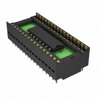
DS1216D Maxim Integrated Products, DS1216D Datasheet
DS1216D
Specifications of DS1216D
Available stocks


Related parts for DS1216D

DS1216D Summary of contents
Page 1
... ORDERING INFORMATION PART TEMP RANGE DS1216B 0°C to +70°C DS1216C 0°C to +70°C DS1216D 0°C to +70°C DS1216E 0°C to +70°C DS1216F 0°C to +70°C DS1216H 0°C to +70°C (See Figure 2 for letter suffix marking identification.) Selector Guide appears on page 2. ...
Page 2
... Write Enable Swi CC M Switched Switched Low [A2 [A0 DQ0 GND 16 32-Pin PC BOARD MODIFICATION RAM DE NSITY REQUIRED FOR DENSITY 16k/64k 64k/256k 256k/1M 64k/256k 64k/256k/1M 1M/ tive Low tched V for 28-/32-Pin RAM CC for 24 -Pin RAM 28-Pin RAM DS1216D/F/H Intelligent Socket UPGRADE? No/Yes No No/Yes ...
Page 3
DE AILED DESC T RIPTION The DS1216 SmartWatch RA built-in CMOS watch function The sockets provide an NV RAM so from 26 pins to 32 pins. When a socket is m problems associated with memory vola The SmartWatch ...
Page 4
If a match is not found, the pointe and all subsequent write cycles are ignored read cycle occurs at any time during p the present sequence is aborted and the ...
Page 5
Figure 1. SmartWatch Comparison Register Definition 7 1 BYTE 0 0 BYTE 1 1 BYTE 2 0 BYTE 3 1 BYTE 4 0 BYTE 5 1 BYTE BYTE 7 NOTE: THE PATTERN RECOGNITION IN HEX IS C5, ...
Page 6
SMARTWATCH REGISTER INFORMATION The SmartWatch information is contained in eight registers of 8 bits, each of which is sequentially accessed one after the 64-bit p ttern t ti updating the S mar tW atch registers, ...
Page 7
... In this case, the socket will ignore the RST input, preventing address transitions from resetting the pattern match, even if the RST bit is enabled. On the DS1216B and DS1216D, the two V V from the controller is connected to the two V CC modifications are required if the lower density RAM is used ...
Page 8
Figure 3. SmartWatch Register Definition REGISTER 12/ 0.1 SEC 0.01 SEC 10 SEC SECONDS 10 MIN MINUTES 0 10 ...
Page 9
ABSOLUTE MAXIMUM RATINGS Voltage Range on any Pin Relative to Ground…………………………………………….…………-0.3V to +7.0V for 5V Operating Temperature Range………………………………………………… Storage Temperature Range……………………………………………………………………………..…...-40°C to +70°C Soldering Temperature Range………………………………………………...….See J-STD-020A Specification (Note 6) This is a stre ss rating only and functional operation ...
Page 10
CAPACITANCE (T = +25C) A PARAMETER Input Capacitance Output Capacitance Expected Data Retention AC EL ECTRICAL CHARAC ( .5V to 5.5V 0° PARAMETER Read Cycle Time CE Ac cess Time OE Access ...
Page 11
Timing D iagram: Read Cycle to SmartWatch Timing Diag ram: Write Cycle to SmartWatch DS1216 SmartWatch RAM/SmartWatch ROM ...
Page 12
Timing Diagram: Reset for SmartWatch Timing Diagram: Power-Down (U) V (L) CC *Note 1 Timing Diag ram: Power-Up DS1216 SmartWatch RAM/SmartWatch ROM ...
Page 13
WARNING: Under no circumstances should negative undershoots of any amplitude be allowed when the devi battery-backup mode. Water washing for flux removal will discharge internal lithium source because exposed voltage pins are present. NOTES: 1) Pin locations are designated “U” ...
Page 14
... IN. 0.090 0.110 0.090 0.110 MM H IN. 0.590 0.630 0.590 0.630 IN. 0.015 0.021 IN. MM © 2004 Maxim Integrated Products ackage outline 28-PIN 32-PIN MIN MAX MIN MAX 35.31 36.07 40.13 41.14 0.720 17.53 18.29 17 .53 18.29 0.470 10.67 11.94 10 ...