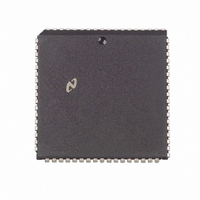
DP8421AV-25 National Semiconductor, DP8421AV-25 Datasheet - Page 25

DP8421AV-25
Manufacturer Part Number
DP8421AV-25
Description
IC CTRLR/DVR CMOS PROGRAM 68PLCC
Manufacturer
National Semiconductor
Datasheet
1.DP8420AV-25.pdf
(58 pages)
Specifications of DP8421AV-25
Controller Type
Dynamic RAM (DRAM)
Voltage - Supply
4.5 V ~ 5.5 V
Operating Temperature
0°C ~ 70°C
Package / Case
68-PLCC
Lead Free Status / RoHS Status
Contains lead / RoHS non-compliant
Other names
*DP8421AV-25
Available stocks
Company
Part Number
Manufacturer
Quantity
Price
Company:
Part Number:
DP8421AV-25
Manufacturer:
Texas Instruments
Quantity:
10 000
Part Number:
DP8421AV-25
Manufacturer:
NS/国半
Quantity:
20 000
5 0 Refresh Options
5 2 REFRESH CYCLE TYPES
Three different types of refresh cycles are available for use
The three different types are mutually exclusive and can be
used with any of the three modes of refresh control The
three different refresh cycle types are all RAS refresh stag-
gered RAS refresh and error scrubbing during all RAS re-
fresh In all refresh cycle types the RAS precharge time is
guaranteed between the previous access RAS ending and
the refresh RAS0 starting between refresh RAS3 ending
and access RAS beginning between burst refresh RASs
5 2 2 Staggered RAS Refresh
A staggered refresh staggers each RAS or group of RASs
by a positive edge of CLK as shown in Figure 17 The num-
ber of RASs which will be asserted on each positive edge
of CLK is determined by the RAS CAS configuration mode
programming bits C4–C6 If single RAS outputs are select-
ed during programming then each RAS will assert on suc-
cessive positive edges of CLK If two RAS outputs are se-
lected during programming then RAS0 and RAS1 will assert
(Continued)
FIGURE 16 Conventional RAS Refresh
FIGURE 17 Staggered RAS Refresh
25
5 2 1 Conventional RAS Refresh
A conventional refresh cycle causes RAS0– 3 to all assert
from the first positive edge of CLK after RFIP is asserted as
shown in Figure 16 RAS0– 3 will stay asserted until the
number of positive edges of CLK programmed have passed
On the last positive edge RAS0– 3 and RFIP will be negat-
ed This type of refresh cycle is programmed by negating
address bit R9 during programming
on the first positive edge of CLK after RFIP is asserted
RAS2 and RAS3 will assert on the second positive edge of
CLK after RFIP is asserted If all RAS outputs were selected
during programming all RAS outputs would assert on the
first positive edge of CLK after RFIP is asserted Each RAS
or group of RASs will meet the programmed RAS low time
and then negate
TL F 8588 – 69
TL F 8588 – 70


