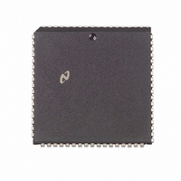
DP8421AV-25 National Semiconductor, DP8421AV-25 Datasheet - Page 43

DP8421AV-25
Manufacturer Part Number
DP8421AV-25
Description
IC CTRLR/DVR CMOS PROGRAM 68PLCC
Manufacturer
National Semiconductor
Datasheet
1.DP8420AV-25.pdf
(58 pages)
Specifications of DP8421AV-25
Controller Type
Dynamic RAM (DRAM)
Voltage - Supply
4.5 V ~ 5.5 V
Operating Temperature
0°C ~ 70°C
Package / Case
68-PLCC
Lead Free Status / RoHS Status
Contains lead / RoHS non-compliant
Other names
*DP8421AV-25
Available stocks
Company
Part Number
Manufacturer
Quantity
Price
Company:
Part Number:
DP8421AV-25
Manufacturer:
Texas Instruments
Quantity:
10 000
Part Number:
DP8421AV-25
Manufacturer:
NS/国半
Quantity:
20 000
Number
1
2
3 4
5
6
7 8
9a
9b
9c
9d
10a
10b
11a
11b
12
13
14
15
16
17
18
19
20
13 0 AC Timing Parameters
Unless otherwise stated V
per bank including trace capacitance (Note 2)
Two different loads are specified
C
C
L
L
e
e
50 pF loads on all outputs except
150 pF loads on Q0–8 9 10 and WE or
f
tCLKP
tCLKPW
fDCLK
tDCLKP
tDCLKPW
tPRASCAS0 RAS Asserted to CAS Asserted
tPRASCAS1 RAS Asserted to CAS Asserted
tPRASCAS2 (RAS Asserted to CAS Asserted
tPRASCAS3 (RAS Asserted to CAS Asserted
tRAH
tRAH
tASC
tASC
tPCKRAS
tPARQRAS
tPENCL
tPENCH
tPARQCAS
tPCLKWH
tPCLKDL0
tPEWL
tSECK
CLK
Symbol
CLK Frequency
CLK Period
CLK Pulse Width
DELCLK Frequency
DELCLK Period
DELCLK Pulse Width
(tRAH
(tRAH
(tRAH
(tRAH
Row Address Hold Time (tRAH
Row Address Hold Time (tRAH
Column Address Setup Time (tASC
Column Address Setup Time (tASC
CLK High to RAS Asserted
following Precharge
AREQ Negated to RAS Negated
ECAS0–3 Asserted to CAS Asserted
ECAS0–3 Negated to CAS Negated
AREQ Negated to CAS Negated
CLK to WAIT Negated
CLK to DTACK Asserted
(Programmed as DTACK of 1 2 1 1
or if WAITIN is Asserted)
ECAS Negated to WAIT Asserted
during a Burst Access
ECAS Asserted Setup to CLK High to
Recognize the Rising Edge of CLK
during a Burst Access
CC
e
e
e
e
e
5 0V
15 ns tASC
15 ns tASC
25 ns tASC
25 ns tASC
Common Parameter
g
Description
10% 0 C
e
e
e
e
(Continued)
0 ns)
10 ns)
0 ns)
10 ns)
k
T
A k
e
e
15)
25)
70 C the output load capacitance is typical for 4 banks of 18 DRAMs
e
e
0)
10)
43
C
C
C
Min
H
H
H
50
15
50
15
30
40
40
50
15
25
10
24
0
5
0
e
e
e
8420A 21A 22A-20
C
50 pF loads on all outputs except
125 pF loads on RAS0– 3 and CAS0–3 and
380 pF loads on Q0– 8 9 10 and WE
L
Max
200
20
20
27
38
23
25
60
39
33
44
Min
50
15
50
15
30
40
40
50
15
25
10
24
0
5
0
C
H
Max
200
20
20
32
43
31
33
68
39
33
44
Min
40
12
50
12
30
40
40
50
15
25
10
19
0
5
0
8420A 21A 22A-25
C
L
Max
200
25
20
22
31
20
20
47
31
28
36
Min
40
12
50
12
30
40
40
50
15
25
10
19
0
5
0
C
H
Max
200
25
20
26
35
27
27
54
31
28
36


