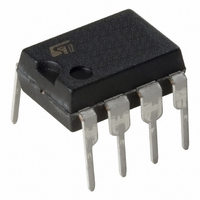
L6590AN STMicroelectronics, L6590AN Datasheet - Page 12

L6590AN
Manufacturer Part Number
L6590AN
Description
IC SWIT OVP OCP 8DIP
Manufacturer
STMicroelectronics
Datasheet
1.L6590AN.pdf
(19 pages)
Specifications of L6590AN
Output Isolation
Isolated
Frequency Range
52 ~ 74kHz
Voltage - Input
6.6 ~ 17.5 V
Voltage - Output
700V
Power (watts)
15W
Operating Temperature
-40°C ~ 150°C
Package / Case
8-DIP (0.300", 7.62mm)
Output Voltage
700 V
Output Current
0.7 A
Output Power
15 W
Input Voltage
6.6 V to 17.5 V
Operating Temperature Range
- 40 C to + 150 C
Mounting Style
Through Hole
Duty Cycle (max)
73 %
Lead Free Status / RoHS Status
Lead free / RoHS Compliant
Other names
497-4807-5
Available stocks
Company
Part Number
Manufacturer
Quantity
Price
Company:
Part Number:
L6590AN
Manufacturer:
STMicroelectronics
Quantity:
1 780
L6590A
APPLICATION INFORMATION
In the following sections the functional blocks as well as the most important internal functions of the device will
be described.
Start-up circuit
When power is first applied to the circuit and the voltage on the bulk capacitor is sufficiently high, an internal
high-voltage current generator is sufficiently biased to start operating and drawing about 4.5 mA through the
primary winding of the transformer and the drain pin. Most of this current charges the bypass capacitor connect-
ed between pin Vcc (3) and ground and makes its voltage rise linearly.
As the Vcc voltage reaches the start-up threshold (14.5V typ.) the chip, after resetting all its internal logic, starts
operating, the internal power MOSFET is enabled to switch and the internal high-voltage generator is discon-
nected. The IC is powered by the energy stored in the Vcc capacitor until the self-supply circuit (typically an
auxiliary winding of the transformer) develops a voltage high enough to sustain the operation.
As the IC is running, the supply voltage, typically generated by a self-supply winding, can range between 16 V
(Overvoltage protection limit, see the relevant section) and 7 V, threshold of the Undervoltage Lockout. Below
this value the device is switched off (and the internal start-up generator is activated). The two thresholds are in
tracking.
The voltage on the Vcc pin is limited at safe values by a clamp circuit. Its 17V threshold tracks the Overvoltage
protection threshold.
Figure 26. Start-up circuit internal schematic
DRAIN
POWER
MOSFET
15 M
UVLO
Vcc
150
17 V
L6590A
GND
Power MOSFET and Gate Driver
The power switch is implemented with a lateral N-channel MOSFET having a V
of 700V min. and a typ-
(BR)DSS
ical RDS(on) of 13 . It has a SenseFET structure to allow a virtually lossless current sensing (used only for
protection).
During operation in Discontinuous Conduction Mode at low mains the drain voltage is likely to go below ground.
Any risk of injecting the substrate of the IC is prevented by an internal structure surrounding the switch.
The gate driver of the power MOSFET is designed to supply a controlled gate current during both turn-on and
turn-off in order to minimize common mode EMI.
Under UVLO conditions an internal pull-down circuit holds the gate low in order to ensure that the power MOS-
FET cannot be turned on accidentally.
12/19


