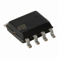
TSM1012IDT STMicroelectronics, TSM1012IDT Datasheet - Page 5

TSM1012IDT
Manufacturer Part Number
TSM1012IDT
Description
IC CTRLR BATT CHRGR/ADAPT 8-SOIC
Manufacturer
STMicroelectronics
Datasheet
1.TSM1012AIST.pdf
(8 pages)
Specifications of TSM1012IDT
Function
Charge Management
Battery Type
All Battery Types
Voltage - Supply
4.5 V ~ 28 V
Operating Temperature
-40°C ~ 105°C
Mounting Type
Surface Mount
Package / Case
8-SOIC (0.154", 3.90mm Width)
Product
Charge Management
Output Current
10 mA
Operating Supply Voltage
4.5 V to 28 V
Maximum Operating Temperature
+ 105 C
Minimum Operating Temperature
- 40 C
Mounting Style
SMD/SMT
Lead Free Status / RoHS Status
Lead free / RoHS Compliant
Other names
497-6623-2
TSM1012IDT
TSM1012IDT
Available stocks
Company
Part Number
Manufacturer
Quantity
Price
1. Voltage and Current Control
1.1. Voltage Control
The voltage loop is controlled via a first transcon-
ductance operational amplifier, the resistor bridge
R1, R2, and the optocoupler which is directly con-
nected to the output.
The relation between the values of R1 and R2
should be chosen as written in Equation 1.
R1 = R2 x Vref / (Vout - Vref)
Where Vout is the desired output voltage.
To avoid the discharge of the load, the resistor
bridge R1, R2 should be highly resistive. For this
type of application, a total value of 100K
more) would be appropriate for the resistors R1
and R2.
As an example, with R2 = 100K , Vout = 4.10V,
Vref = 1.210V, then R1 = 41.9K .
Note that if the low drop diode should be inserted
between the load and the voltage regulation resis-
tor bridge to avoid current flowing from the load
through the resistor bridge, this drop should be
taken into account in the above calculations by re-
placing Vout by (Vout + Vdrop).
1.2. Current Control
The current loop is controlled via the second
trans-conductance
sense resistor Rsense, and the optocoupler.
Vsense threshold is achieved externally by a re-
sistor bridge tied to the Vref voltage reference. Its
middle point is tied to the positive input of the cur-
rent control operational amplifier, and its foot is to
be connected to lower potential point of the sense
resistor as shown on the following figure. The re-
sistors of this bridge are matched to provide the
best precision possible
The control equation verifies:
Rsense x Ilim = Vsense
Vsense = R5*Vref/(R4+R5)
Ilim = R5*Vref/(R4+R5)*Rsense
where Ilim is the desired limited current, and
Vsense is the threshold voltage for the current
control loop.
PRINCIPLE OF OPERATION AND APPLICATION HINTS
operational
amplifier,
eq2'
eq2
Eq1
the
(or
Note that the Rsense resistor should be chosen
taking into account the maximum dissipation
(Plim) through it during full load operation.
Plim = Vsense x Ilim.
Therefore, for most adapter and battery charger
applications, a quarter-watt, or half-watt resistor to
make the current sensing function is sufficient.
The current sinking outputs of the two trans-con-
nuctance operational amplifiers are common (to
the output of the IC). This makes an ORing func-
tion which ensures that whenever the current or
the voltage reaches too high values, the optocou-
pler is activated.
The relation between the controlled current and
the controlled output voltage can be described
with a square characteristic as shown in the fol-
lowing V/I output-power graph.
Figure 3 : Output voltage versus output current
2. Compensation
The voltage-control trans-conductance operation-
al amplifier can be fully compensated. Both of its
output and negative input are directly accessible
for external compensation components.
An example of a suitable compensation network is
shown in Fig.2. It consists of a capacitor
Cvc1=2.2nF and a resistor Rcv1=22K
0
TSM1012 Vcc : independent power supply
Secondary current regulation
Vout
Voltage regulation
TSM1012 Vcc : On power output
Primary current regulation
TSM1012
eq3
in series.
Iout
5/8


