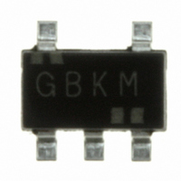
S-8241ABKMC-GBKT2G Seiko Instruments, S-8241ABKMC-GBKT2G Datasheet - Page 15

S-8241ABKMC-GBKT2G
Manufacturer Part Number
S-8241ABKMC-GBKT2G
Description
IC BATT PROTECTION 1CELL SOT23-5
Manufacturer
Seiko Instruments
Datasheet
1.S-8241ABPMC-GBPT2G.pdf
(38 pages)
Specifications of S-8241ABKMC-GBKT2G
Function
Over/Under Voltage Protection
Battery Type
Lithium-Ion (Li-Ion), Lithium-Polymer (Li-Pol)
Operating Temperature
-40°C ~ 85°C
Mounting Type
Surface Mount
Package / Case
SC-74A, SOT-753
Product
Li-Ion Protection
Output Voltage
8 V
Operating Supply Voltage
1.5 V to 8 V
Supply Current
5 uA
Maximum Operating Temperature
+ 85 C
Minimum Operating Temperature
- 40 C
Mounting Style
SMD/SMT
Uvlo Start Threshold
1 V
Uvlo Stop Threshold
0.4 V
Lead Free Status / RoHS Status
Lead free / RoHS Compliant
Other names
728-1032-2
Available stocks
Company
Part Number
Manufacturer
Quantity
Price
Company:
Part Number:
S-8241ABKMC-GBKT2G
Manufacturer:
SEIKO
Quantity:
12 123
Part Number:
S-8241ABKMC-GBKT2G
Manufacturer:
SII/精工
Quantity:
20 000
Rev.9.0
Caution Unless otherwise specified, the output voltage levels “H” and “L” at CO pin (V
(1) Test Condition 1, Test Circuit 1
(2) Test Condition 2, Test Circuit 1
(3) Test Condition 3, Test Circuit 1
(4) Test Condition 4, Test Circuit 1
Test Circuits
(Overcharge detection voltage, Overcharge release voltage, Overdischarge detection voltage, Overdischarge
release voltage)
(Overcurrent 1 detection voltage, Overcurrent 2 detection voltage, Load short-circuiting detection voltage)
(Charger detection voltage, ( = abnormal charge current detection voltage) )
(Normal operation current consumption, Power-down current consumption, Overdischarge current
consumption)
The overcharge detection voltage (V
when the voltage V1 is gradually increased from the normal condition V1 = 3.5 V and V2 = 0 V. The overcharge release
voltage (V
then gradually decreased.
Gradually decreasing the voltage V1, the overdischarge detection voltage (V
and VSS at which V
VDD and VSS at which V
The overcurrent 1 detection voltage (V
“H” when the voltage V2 is gradually increased from the normal condition V1 = 3.5 V and V2 = 0 V.
The overcurrent 2 detection voltage (V
“H” when the voltage V2 is increased at the speed between 1 ms and 4 ms from the normal condition V1 = 3.5 V and V2
= 0 V.
The load short-circuiting detection voltage (V
“L” from “H” when the voltage V2 is increased at the speed between 1 μs and 50 μs from the normal condition V1 = 3.5
V and V2 = 0 V.
• Applied only for products with overdischarge hysteresis
• Applied only for products without overdischarge hysteresis
Set V1 = 3.5 V and V2 = 0 V under normal condition. The current I
consumption current (I
• For products with power-down function
• For products without power-down function
Set V1 = 1.8 V and V2 = 0 V under overdischarge condition. Increase V1 gradually, set V1 = (V
overdischarge hysteresis, overdischarge condition), then decrease V2 from 0 V gradually. The voltage between VM
and VSS at which V
Set V1 = 3.5 V and V2 = 0 V under normal condition. Decrease V2 from 0 V gradually. The voltage between VM and
VSS at which V
detection voltage has the same value as the charger detection voltage (V
Set V1 = V2 = 1.5 V under overdischarge condition. The current I
current consumption (I
Set V1 = V2 = 1.5 V under overdischarge condition. The current I
current consumption (I
_00
judged by the threshold voltage (1.0 V) of the N-channel FET. Judge the CO pin level with respect to V
and the DO pin level with respect to V
CL
) is defined by the voltage between VDD and VSS at which V
CO
DO
goes “L” from “H” is the abnormal charge current detection voltage. The abnormal charge current
OPE
DO
goes “L” from “H”. The overdischarge release voltage (V
DO
PDN
OPED
goes “H” from “L” is the charger detection voltage (V
).
goes “H” from “L” when the voltage V1 is then gradually increased.
).
).
CU
IOV1
IOV2
) is defined by the voltage between VDD and VSS at which V
) is defined by the voltage between VDD and VSS at which V
) is defined by the voltage between VDD and VSS at which V
Seiko Instruments Inc.
SHORT
SS
BATTERY PROTECTION IC FOR 1-CELL PACK
.
) is defined by the voltage between VDD and VSS at which V
DD
DD
flowing through VDD pin is the normal operation
DD
flowing through VDD pin is the overdischarge
CO
flowing through VDD pin is the power-down
goes “H” from “L” when the voltage V1 is
DL
CHA
) is defined by the voltage between VDD
CHA
).
DU
).
) is defined by the voltage between
CO
) and DO pin (V
S-8241 Series
CO
DU
goes “L” from “H”
DO
DO
+V
goes “L” from
goes “L” from
DL
) / 2 (within
DO
DO
goes
) are
15
VM


