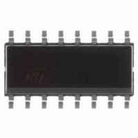
HCF4056M013TR STMicroelectronics, HCF4056M013TR Datasheet - Page 2

HCF4056M013TR
Manufacturer Part Number
HCF4056M013TR
Description
IC DECODER/DIVDR BCD-7SEG 16SOIC
Manufacturer
STMicroelectronics
Datasheet
1.HCF4056M013TR.pdf
(10 pages)
Specifications of HCF4056M013TR
Display Type
LCD
Configuration
7 Segment
Interface
BCD
Digits Or Characters
1 Digit
Voltage - Supply
3 V ~ 20 V
Operating Temperature
-55°C ~ 125°C
Mounting Type
Surface Mount
Package / Case
16-SOIC (3.9mm Width)
Lead Free Status / RoHS Status
Lead free / RoHS Compliant
Current - Supply
-
Other names
497-1132-2
Available stocks
Company
Part Number
Manufacturer
Quantity
Price
Company:
Part Number:
HCF4056M013TR
Manufacturer:
ON
Quantity:
50
HCF4056B
When the DF input is low, the output segments will
be high when selected by the BCD inputs. When
the DF input is high, the output segments will be
low when selected by the BCD inputs. When a
square wave is present at the DF input, the
selected segments will have a square wave output
that is 180 out of phase with the DF input. Those
segments which are not selected will have a
square wave output that is in phase with the input.
DF square wave repetition rates for liquid crystal
displays usually range from 30Hz (well above
flicker rate) to 200Hz (well below the upper limit of
the liquid crystal frequency response). HCF4056B
provides a strobed-latch function at the BCD
inputs. The decoding of all input combinations in
INPUT EQUIVALENT CIRCUIT
FUNCTIONAL DIAGRAM
2/10
this device provides displays of 0 to 9 as well as L,
P, H, A, -, and a blank position. The level shifted
function permits the use of different input and
output signal swings. The input swings from a low
level of V
outputs swing from a low level of V
high level of V
swings can be selected independently of each
other over a 3 to 18V range. V
connected to V
required. The HCF4056B, however must be used
together with HCF4054B to provide the common
DF output.
PIN DESCRIPTION
9, 10, 11, 12,
13, 15, 14
5, 3, 2, 4
PIN No
16
6
1
7
8
SS
2
to a high level of V
0
FREQ. IN
SYMBOL
DISPLAY
STROBE
EE
, 2
DD
a to g
V
V
V
1
, 2
. Thus, the input and output
EE
SS
DD
when no level-shift function is
2
, 2
3
BCD Inputs
7 - Segments Outputs
Display Frequency Input
Strobe Input
Negative Supply Voltage
Negative Supply Voltage
Positive Supply Voltage
NAME AND FUNCTION
EE
DD,
SS
to the same
while the
may be


