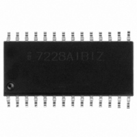
ICM7228AIBIZ Intersil, ICM7228AIBIZ Datasheet - Page 11

ICM7228AIBIZ
Manufacturer Part Number
ICM7228AIBIZ
Description
IC DRIVER DECODER 8DGT CA 28SOIC
Manufacturer
Intersil
Datasheet
1.ICM7228AIBIZ.pdf
(18 pages)
Specifications of ICM7228AIBIZ
Display Type
LED
Configuration
7 Segment
Digits Or Characters
8 Digits
Current - Supply
200µA
Voltage - Supply
4 V ~ 6 V
Operating Temperature
-40°C ~ 85°C
Mounting Type
Surface Mount
Package / Case
28-SOIC (7.5mm Width)
Lead Free Status / RoHS Status
Lead free / RoHS Compliant
Interface
-
Available stocks
Company
Part Number
Manufacturer
Quantity
Price
Company:
Part Number:
ICM7228AIBIZ
Manufacturer:
Intersil
Quantity:
500
Sequential 8-Digit Update
The logic state of DATA COMING (lD7) is also latched
during a Control Register update. If the latched value of
DATA COMING (lD7) is high, the display becomes blanked
and a sequential 8-digit update is initiated. Display data can
now be written into RAM with 8 successive WRITE pulses,
starting with digit 1 and ending with digit 8 (See Figure 2).
After all 8 RAM locations have been written to, the display
turns on again and the new data is displayed. Additional
write pulses are ignored until a new Control Register update
is performed. All 8 digits are displayed in the format
(Hex/Code B or No Decode) specified by the control word
that preceded the 8 digit update. If a decoding scheme
(Hex/Code B) is to be used, the value of lD3 during the
control word update determines which RAM bank will be
written to.
System Interfacing, ICM7228C
The ICM7228C is directly compatible with the architecture of
most microprocessor systems. Its fast switching
characteristics make it possible to access them as a memory
mapped I/O device with no wait state necessary in most
microcontroller systems. All the ICM7228C inputs, excluding
HEXA/CODE B/SHUTDOWN, feature a 250ns minimum
1D2
0
0
0
0
1
1
1
1
INPUT DATA LINES
TABLE 4. DIGITS ADDRESS, ICM7228A/B
I/O OR
MEMORY
WRITE PULSE
lD2
0
0
1
1
0
0
1
1
A1-A15
lD0
11
0
1
0
1
0
1
0
1
FIGURE 9. ICM7228A/B MICROPROCESSOR SYSTEM INTERFACING
DECODER
ENABLE
ADDRESS BUS A0 - A15
DECODER
ADDRESS
SELECTED DIGIT
DATA BUS D0-D7
DIGIT 5
DlGlT 1
DlGlT 2
DIGlT 3
DlGlT 4
DlGlT 6
DlGlT 7
DlGlT 8
DEVICE SELECT
WRITE PULSE
AND
D0 - D7
ICM7228
A0
Single Digit Update
In this mode each digit data in the display RAM can be updated
individually without changing the other display data. First, with
MODE input high, a control word is written to the Control
Register carrying the following information; DATA COMING
(lD7) low, the desired display format data on lD4 - lD6, the RAM
bank selected by lD3 (if decoding is selected) and the address
of the digit to be updated on data lines lD0 - lD2 (See Table 4).
A second write to the ICM7228A/B, this time with MODE input
low, transfers the data at the lD0 - lD7 inputs into the selected
digit’s RAM location. In single digit update mode, each
individual digit’s data can be specified independently for being
displayed in Decoded or No-Decode mode. For those digits
which decoding scheme (Hex/Code B) is selected, only one
can be effective at a time. Whenever a control word is written,
the specified decoding scheme will be applied to all those digits
which selected to be displayed in Decoded mode.
setup and 0ns hold time with a 200ns minimum WRITE pulse.
Input logic levels are TTL and CMOS compatible. Figure 10
shows a generic method of driving the ICM7228C from a
microprocessor bus. To the microprocessor, the 8 bytes of the
Display RAM appear to be 8 separate I/O locations. Loading
the ICM7228C is quite similar to a standard memory write
cycle. The address of the digit to be updated is placed on lines
DA0 - DA2, the data to be written is placed on lines ID0 - lD3
and ID7, then a low pulse on WRITE input will transfer the
data in. See Figure 3 and Switching Characteristics Table for
write cycle timing parameters.
The ICM7228C does not have any control register, and also
does not provide the No Decode display format. Hexadecimal
or Code B character selection and shutdown mode are directly
controlled through the three level input at Pin 9, which is
accordingly called HEXA/CODE B/SHUTDOWN. See Table 3
for input and output definitions of the ICM7228C.
ID0
ID7
WRITE
MODE
ICM7228A/B
INTERSIL
SEGMENTS
DIGITS
DRIVE
DRIVE
LED DISPLAY


