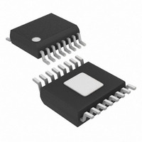
MAX6950EEE+ Maxim Integrated Products, MAX6950EEE+ Datasheet - Page 16

MAX6950EEE+
Manufacturer Part Number
MAX6950EEE+
Description
IC DRVR DSPL LED SRL 16-QSOP
Manufacturer
Maxim Integrated Products
Datasheet
1.MAX6950CEE.pdf
(19 pages)
Specifications of MAX6950EEE+
Display Type
LED
Configuration
7 Segment
Interface
3-Wire Serial
Digits Or Characters
5 Digits
Current - Supply
10mA
Voltage - Supply
2.7 V ~ 5.5 V
Operating Temperature
-40°C ~ 85°C
Mounting Type
Surface Mount
Package / Case
16-QSOP Exposed Pad, 16-eQSOP , 16-HQSOP
Number Of Digits
5
Number Of Segments
40
Low Level Output Current
400 mA
High Level Output Current
- 50 mA
Operating Supply Voltage
2.7 V to 5.5 V
Maximum Supply Current
15 mA
Maximum Power Dissipation
667 mW
Maximum Operating Temperature
+ 85 C
Mounting Style
SMD/SMT
Minimum Operating Temperature
- 40 C
Lead Free Status / RoHS Status
Lead free / RoHS Compliant
be unable to regulate the current correctly. As the sup-
ply voltage drops further, the LED segment drive cur-
rent becomes effectively limited by the output drivers'
on-resistance, and the LED drive current drops. The
characteristics of each individual LED in a modern 7-
segment digit usually match well, so the result is that
the display intensity dims uniformly as supply voltage
drops out of regulation and beyond. The MAX6950/
MAX6951 operate down to 2V supply voltage (although
most displays are very dim at this voltage), providing
that the MAX6950/MAX6951 are powered up initially to
at least 2.7V to trigger the device's internal reset, and
also that the SPI interface is constrained to 5Mbps.
The upper limit for power dissipation (PD) for the
MAX6950/MAX6951 is determined from the following
equation:
Where:
Serially Interfaced, +2.7V to +5.5V,
5- and 8-Digit LED Display Drivers
Table 17. Digit Register Mapping with
Blink Globally Disabled
Table 18. Digit Register Mapping with
Blink Globally Enabled
16
BIT SETTING
IN PLANE P1
BIT SETTING
IN PLANE P1
SEGMENT’S
SEGMENT’S
P
______________________________________________________________________________________
D
X
X
0
0
1
1
= (V+ x I+) + (V+ - V
BIT SETTING
BIT SETTING
IN PLANE P0
IN PLANE P0
SEGMENT’S
SEGMENT’S
Computing Power Dissipation
0
1
0
1
0
1
LED
) (DUTY
Segment off during both
halves of each blink
period
Segment off during both
halves of each blink
period
Segment off
Segment on only during
the 1st half of each blink
period
Segment on only during
the 2nd half of each blink
period
Segment on
BEHAVIOR
BEHAVIOR
SEGMENT
SEGMENT
✕
I
SEG
✕
N)
V+ = supply voltage
DUTY = duty cycle set by intensity register
N = number of segment driven (worst case is 8)
V
I
PD = power dissipation, in mW if currents are in mA
Dissipation example:
P
Thus, for the 16-pin QSOP package (T
+120°C/W), the maximum allowed ambient temperature
T
T
So T
safely at a maximum package temperature of +85°C.
The MAX6950/MAX6951 operate from a single +2.7V to
+5.5V power supply. Bypass the power supply to
ground with a 0.1µF capacitor as close to the pin as
possible. Add a 22µF capacitor if the MAX6950/
MAX6951 are not close to the board’s input bulk decou-
pling capacitor.
Connect the underside exposed pad to GND.
When designing a board, use the following guidelines:
1. The R
2. Ensure that the track from the ground end of R
Figure 5 shows a good layout. The decoupling capaci-
tors C1 (ceramic) and C2 (bulk, if required) are located
above the IC. The ground track to R
track from both the IC's power ground connection and
the ground plane.
SEG
A
J (MAX)
LED
D
I
is given by:
= 3.6V (15mA) + (3.6V - 2.4V)(15 / 16
= 0.414W
SEG
node, and sensitive to layout. Place R
to pins 7 and 8 and route R
with very short tracks.
routes directly to pin 8, and that this track is not
used as part of any other ground connection.
A
= segment current set by R
= LED forward voltage
= +100°C. Thus, the device can be operated
= 40mA, N = 8, Duty = 15/16, V
= T
SET
40mA, V+ = 3.6V
+120°C/W)
A
connection to pin 7 is a high-impedance
+ (P
D
✕
T
JA
) = +150°C = T
SET
SET
directly to these pins
Power Supplies
SET
Board Layout
JA
LED
A
✕
= 1/0.00834 =
SET
is a separate
+ (0.44
40mA x 8)
= 2.4V at
right next
✕
SET


