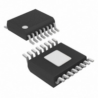
MAX6950EEE+ Maxim Integrated Products, MAX6950EEE+ Datasheet - Page 8

MAX6950EEE+
Manufacturer Part Number
MAX6950EEE+
Description
IC DRVR DSPL LED SRL 16-QSOP
Manufacturer
Maxim Integrated Products
Datasheet
1.MAX6950CEE.pdf
(19 pages)
Specifications of MAX6950EEE+
Display Type
LED
Configuration
7 Segment
Interface
3-Wire Serial
Digits Or Characters
5 Digits
Current - Supply
10mA
Voltage - Supply
2.7 V ~ 5.5 V
Operating Temperature
-40°C ~ 85°C
Mounting Type
Surface Mount
Package / Case
16-QSOP Exposed Pad, 16-eQSOP , 16-HQSOP
Number Of Digits
5
Number Of Segments
40
Low Level Output Current
400 mA
High Level Output Current
- 50 mA
Operating Supply Voltage
2.7 V to 5.5 V
Maximum Supply Current
15 mA
Maximum Power Dissipation
667 mW
Maximum Operating Temperature
+ 85 C
Mounting Style
SMD/SMT
Minimum Operating Temperature
- 40 C
Lead Free Status / RoHS Status
Lead free / RoHS Compliant
The no-op register is used when the MAX6950/
MAX6951 are connected as the last device on a chain
of cascaded SPI devices. To write the other cascaded
device(s), ensure that while the intended device
receives its specific command, the MAX6950/MAX6951
receive a no-op command.
Serially Interfaced, +2.7V to +5.5V,
5- and 8-Digit LED Display Drivers
Table 3. Register Address Map
8
No-Op
Decode Mode
Intensity
Scan Limit
Configuration
Factory reserved. Do not write to this.
Display Test
Digit 0 plane P0 only (plane 1 unchanged)
Digit 1 plane P0 only (plane 1 unchanged)
Digit 2 plane P0 only (plane 1 unchanged)
Digit 3 plane P0 only (plane 1 unchanged)
Digit 4 plane P0 only (plane 1 unchanged)
Digit 5 plane P0 only (plane 1 unchanged)
Digit 6 plane P0 only (plane 1 unchanged)
Digit 7 plane P0 only (plane 1 unchanged)
Digit 0 plane P1 only (plane 0 unchanged)
Digit 1 plane P1 only (plane 0 unchanged)
Digit 2 plane P1 only (plane 0 unchanged)
Digit 3 plane P1 only (plane 0 unchanged)
Digit 4 plane P1 only (plane 0 unchanged)
Digit 5 plane P1 only (plane 0 unchanged)
Digit 6 plane P1 only (plane 0 unchanged)
Digit 7 plane P1 only (plane 0 unchanged)
D i g i t 0 p l ane P 0 and p l ane P 1 ( w i th sam e d ata)
D i g i t 1 p l ane P 0 and p l ane P 1 ( w i th sam e d ata)
D i g i t 2 p l ane P 0 and p l ane P 1 ( w i th sam e d ata)
D i g i t 3 p l ane P 0 and p l ane P 1 ( w i th sam e d ata)
D i g i t 4 p l ane P 0 and p l ane P 1 ( w i th sam e d ata)
D i g i t 5 p l ane P 0 and p l ane P 1 ( w i th sam e d ata)
D i g i t 6 p l ane P 0 and p l ane P 1 ( w i th sam e d ata)
D i g i t 7 p l ane P 0 and p l ane P 1 ( w i th sam e d ata)
_______________________________________________________________________________________
REGISTER
No-Op Register
D15
0
0
0
0
0
0
0
0
0
0
0
0
0
0
0
0
0
0
0
0
0
0
0
0
0
0
0
0
0
0
0
D14
0
0
0
0
0
0
0
0
0
0
0
0
0
0
0
1
1
1
1
1
1
1
1
1
1
1
1
1
1
1
1
The display-test register switches the drivers between
one of two modes: normal and display test. Display-test
mode turns all LEDs on by overriding, but not altering,
all control and digit registers (including the Shutdown
register) In display-test mode, eight digits are scanned
and the duty cycle is 7/16 (half power). Table 11 lists
the display-test register format.
D13
0
0
0
0
0
0
0
1
1
1
1
1
1
1
1
0
0
0
0
0
0
0
0
1
1
1
1
1
1
1
1
COMMAND ADDRESS
D12
0
0
0
0
0
0
0
0
0
0
0
0
0
0
0
0
0
0
0
0
0
0
0
0
0
0
0
0
0
0
0
D11
0
0
0
0
0
0
0
0
0
0
0
0
0
0
0
0
0
0
0
0
0
0
0
0
0
0
0
0
0
0
0
D10
0
0
0
0
1
1
1
0
0
0
0
1
1
1
1
0
0
0
0
1
1
1
1
0
0
0
0
1
1
1
1
Display-Test Register
D9
0
0
1
1
0
1
1
0
0
1
1
0
0
1
1
0
0
1
1
0
0
1
1
0
0
1
1
0
0
1
1
D8
0
1
0
1
0
0
1
0
1
0
1
0
1
0
1
0
1
0
1
0
1
0
1
0
1
0
1
0
1
0
1
CODE
HEX
0x00
0x01
0x02
0x03
0x04
0x06
0x07
0x20
0x21
0x22
0x23
0x24
0x25
0x26
0x27
0x40
0x41
0x42
0x43
0x44
0x45
0x46
0x47
0x60
0x61
0x62
0x63
0x64
0x65
0x66
0x67


