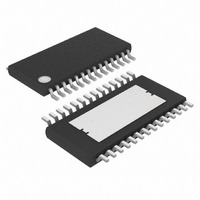
MAX7456EUI+ Maxim Integrated Products, MAX7456EUI+ Datasheet - Page 38

MAX7456EUI+
Manufacturer Part Number
MAX7456EUI+
Description
IC ON-SCREEN DISPLAY 28-TSSOP
Manufacturer
Maxim Integrated Products
Type
OSD (On-Screen Display) Video Generatorr
Datasheet
1.MAX7456EUI.pdf
(44 pages)
Specifications of MAX7456EUI+
Applications
Security Systems, Video Routing
Mounting Type
Surface Mount
Package / Case
28-TSSOP Exposed Pad, 28-eTSSOP, 28-HTSSOP
Current - Supply
58mA
Voltage - Supply
4.75 V ~ 5.25 V
Operating Temperature
-40°C ~ 85°C
Interface
SPI Serial
Display Type
OSD
Digits Or Characters
256 Characters
Maximum Clock Frequency
27 MHz
Operating Supply Voltage
5 V
Maximum Power Dissipation
2162 mW
Maximum Operating Temperature
+ 85 C
Maximum Supply Current
25 mA
Minimum Operating Temperature
- 40 C
Mounting Style
SMD/SMT
Lead Free Status / RoHS Status
Lead free / RoHS Compliant
Configuration
-
Lead Free Status / Rohs Status
Lead free / RoHS Compliant
Single-Channel Monochrome On-Screen
Display with Integrated EEPROM
Only whole characters (54 bytes of pixel data) can be
written to or read from the NVM character memory at one
time. This is done through the (64 byte) shadow RAM
(see Figure 13). The shadow RAM is accessed by the
SPI port one byte at a time. The shadow RAM is written
to and read from the NVM by a single SPI command.
Writing a new character:
1) Write VM0[3] = 0 to disable the OSD image display.
2) Write CMAH[7:0] = xxH to select the character
3) Write CMAL[7:0] = xxH to select the 4-pixel byte
4) Write CMDI[7:0] = xxH to set the pixel values of the
5) Repeat steps 3 and 4 until all 54 bytes of the char-
6) Write CMM[7:0] = 1010xxxx to write to the NVM
7) Write VM0[3] = 1 to enable the OSD image display.
Modifying an existing character:
1) Write VM0[3] = 0 to disable the OSD image display.
2) Write CMAH[7:0] = xxH to select the character
3) Write CMM[7:0] = 0101xxxx to read character data
4) Write CMAL[7:0] = xxH to select the 4-pixel byte
5) Read CMDO[7:0] = xxH to read the byte of 4-pixel
6) Modify the byte of 4-pixel data as desired.
7) Write CMDI[7:0] = xxH to write the modified byte of
8) Repeat steps 4 through 7 as needed until all pixels
9) Write CMM[7:0] = 1010xxxx to write the shadow
38
(0–255) to be written (Figures 10 and 13).
(0–63) in the character to be written (Figures 10 and
13).
selected part of the character (Figures 11 and 13).
acter data are loaded into the shadow RAM.
array from the shadow RAM (Figure 13). The char-
acter memory is busy for approximately 12ms dur-
ing this operation. STAT[5] can be read to verify that
the NVM writing process is complete.
(0–255) to be modified (Figures 10 and 13).
from the NVM to the shadow RAM (Figure 13).
(0–63) in the character to be modified (Figures 10
and 13).
data to be modified (Figures 11 and 13).
4-pixel data back to the shadow RAM (Figures 11
and 13).
have been loaded into the shadow RAM.
RAM data to the NVM (Figure 13). The character
______________________________________________________________________________________
Applications Information
Character-Memory Operation
Steps for Writing Character Bytes
into the NVM Character Memory
10) Write VM0[3] =1 to enable the OSD image display.
1) Write VM0[3] = 0 to disable the OSD image.
2) Write CMAH[7:0] = xxH to select the character
3) Write CMM[7:0] = 0101xxxx to read the character
4) Write CMAL[7:0] = xxH to select the 4-pixel byte
5) Read CMDO[7:0] = xxH to read the selected 4-pixel
6) Repeat steps 4 and 5 to read other bytes of 4-pixel
7) Write VM0[3] = 1 to enable the OSD image display.
The following two steps enable viewing of the OSD
image. These steps are not required to read from or
write to the display memory:
1) Write VM0[3] = 1 to enable the display of the OSD
2) Write OSDBL[4] = 0 to enable automatic OSD black
Write DMM[2] = 1 to start the clear display-memory
operation. This operation typically takes 20µs. The
Display Memory Mode register cannot be written to
again until the clear operation is complete. DMM[2] is
automatically reset to zero upon completion.
The 8-bit operation mode provides maximum flexibility
when writing characters to the display memory. This
mode enables writing individual Character Attribute
bytes for each character (see Table 5). This mode is
distinct from the 16-bit operation mode where the
Character Attribute byte is automatically copied from
DMM[5:3] when a character is written (Figure 19).
Write DMM[6] = 1 to select the 8-bit operation mode.
memory is busy for typically 12ms during this oper-
ation. STAT[5] can be read to verify that the NVM
writing process is complete.
(0–255) to be read (Figures 10 and 13).
data from the NVM to the shadow RAM (Figure 13).
(0–63) in the character to be read (Figures 10 and 13).
byte of data (Figures 11 and 13).
data.
image.
level control. This ensures the correct OSD image
brightness. This register contains 4 factory-preset
bits [3:0] that must not be changed. Therefore,
when changing bit 4, first read OSDBL[7:0], modify
bit 4, and then write back the updated byte.
Steps for Clearing Display Memory
Display-Memory Operation
Bytes from Character Memory
Display Memory in 8-Bit Mode
Steps for Reading Character
Steps for Writing to


