MAX7456EUI+ Maxim Integrated Products, MAX7456EUI+ Datasheet - Page 42
MAX7456EUI+
Manufacturer Part Number
MAX7456EUI+
Description
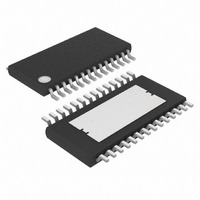
IC ON-SCREEN DISPLAY 28-TSSOP
Manufacturer
Maxim Integrated Products
Type
OSD (On-Screen Display) Video Generatorr
Datasheet
1.MAX7456EUI.pdf
(44 pages)
Specifications of MAX7456EUI+
Applications
Security Systems, Video Routing
Mounting Type
Surface Mount
Package / Case
28-TSSOP Exposed Pad, 28-eTSSOP, 28-HTSSOP
Current - Supply
58mA
Voltage - Supply
4.75 V ~ 5.25 V
Operating Temperature
-40°C ~ 85°C
Interface
SPI Serial
Display Type
OSD
Digits Or Characters
256 Characters
Maximum Clock Frequency
27 MHz
Operating Supply Voltage
5 V
Maximum Power Dissipation
2162 mW
Maximum Operating Temperature
+ 85 C
Maximum Supply Current
25 mA
Minimum Operating Temperature
- 40 C
Mounting Style
SMD/SMT
Lead Free Status / RoHS Status
Lead free / RoHS Compliant
Configuration
-
Lead Free Status / Rohs Status
Lead free / RoHS Compliant


Single-Channel Monochrome On-Screen
Display with Integrated EEPROM
The MAX7456 provides a TTL clock output (CLKOUT)
capable of driving one CLKIN pin of another MAX7456.
Two or more MAX7456 parts can be driven using an
external clock driver. This arrangement reduces the
system cost by having only one crystal on one
MAX7456 that supplies the clock signal to multiple
MAX7456 parts (Figure 25).
Choose a 27MHz parallel resonant, fundamental mode
crystal. No external load capacitors are needed. All
capacitors required for the Pierce oscillator are includ-
ed on-chip.
The MAX7456 operates from three independent supply
lines. Each supply must be within a +4.75V to +5.25V
voltage range. Separate the digital power supply from
the analog and video-driver supply lines to prevent
high-frequency digital noise that may couple onto the
video output. All three supplies should be at the same
DC voltage. Bypass each supply with a 0.1µF capacitor
to ground very close to the IC pins. There are no
power-supply sequencing requirements for the device.
For best performance, make the VIN and VOUT traces
as short as possible. Place all AC-coupling capacitors
and 75Ω termination resistors close to the device with
the resistors terminated to the solid analog ground
plane. Since the MAX7456 TSSOP package has an
exposed pad (EP) underneath, do not run traces under
the package to avoid possible short circuits. Refer to
the MAX7456 EV kit for an example of PCB layout.
To aid heat dissipation, the EP should be connected to
a similarly sized pad on the component side of the
PCB. This pad should be connected through to the sol-
der-side copper by several plated holes to conduct
heat away from the device. The solder-side copper pad
area should be larger than the EP area. It is recom-
mended that the EP be connected to ground, but it is
not required. Do not use EP as the only ground connec-
tion for the device.
42
______________________________________________________________________________________
Power Supply and Bypassing
Common Clock Application
Selecting a Clock Crystal
Multiple OSDs with
Layout Concerns
PROCESS: BiCMOS
TOP VIEW
CLKOUT
SDOUT
CLKIN
DGND
DVDD
SCLK
SDIN
N.C.
N.C.
N.C.
N.C.
XFB
LOS
CS
10
11
12
13
14
1
2
3
4
5
6
7
8
9
+
MAX7456
TSSOP
Pin Configuration
Chip Information
28
27
26
25
24
23
22
21
20
19
18
17
16
15
N.C.
N.C.
VOUT
SAG
PVDD
PGND
VIN
AVDD
AGND
RESET
HSYNC
VSYNC
N.C.
N.C.
Related parts for MAX7456EUI+
Image
Part Number
Description
Manufacturer
Datasheet
Request
R

Part Number:
Description:
MAX7528KCWPMaxim Integrated Products [CMOS Dual 8-Bit Buffered Multiplying DACs]
Manufacturer:
Maxim Integrated Products
Datasheet:
Part Number:
Description:
Single +5V, fully integrated, 1.25Gbps laser diode driver.
Manufacturer:
Maxim Integrated Products
Datasheet:
Part Number:
Description:
Single +5V, fully integrated, 155Mbps laser diode driver.
Manufacturer:
Maxim Integrated Products
Datasheet:
Part Number:
Description:
VRD11/VRD10, K8 Rev F 2/3/4-Phase PWM Controllers with Integrated Dual MOSFET Drivers
Manufacturer:
Maxim Integrated Products
Datasheet:
Part Number:
Description:
Highly Integrated Level 2 SMBus Battery Chargers
Manufacturer:
Maxim Integrated Products
Datasheet:
Part Number:
Description:
Current Monitor and Accumulator with Integrated Sense Resistor; ; Temperature Range: -40°C to +85°C
Manufacturer:
Maxim Integrated Products
Part Number:
Description:
TSSOP 14/A�/RS-485 Transceivers with Integrated 100O/120O Termination Resis
Manufacturer:
Maxim Integrated Products
Part Number:
Description:
TSSOP 14/A�/RS-485 Transceivers with Integrated 100O/120O Termination Resis
Manufacturer:
Maxim Integrated Products
Part Number:
Description:
QFN 16/A�/AC-DC and DC-DC Peak-Current-Mode Converters with Integrated Step
Manufacturer:
Maxim Integrated Products
Part Number:
Description:
TDFN/A/65V, 1A, 600KHZ, SYNCHRONOUS STEP-DOWN REGULATOR WITH INTEGRATED SWI
Manufacturer:
Maxim Integrated Products
Part Number:
Description:
Integrated Temperature Controller f
Manufacturer:
Maxim Integrated Products
Part Number:
Description:
SOT23-6/I�/45MHz to 650MHz, Integrated IF VCOs with Differential Output
Manufacturer:
Maxim Integrated Products
Part Number:
Description:
SOT23-6/I�/45MHz to 650MHz, Integrated IF VCOs with Differential Output
Manufacturer:
Maxim Integrated Products
Part Number:
Description:
EVALUATION KIT/2.4GHZ TO 2.5GHZ 802.11G/B RF TRANSCEIVER WITH INTEGRATED PA
Manufacturer:
Maxim Integrated Products
Part Number:
Description:
QFN/E/DUAL PCIE/SATA HIGH SPEED SWITCH WITH INTEGRATED BIAS RESISTOR
Manufacturer:
Maxim Integrated Products
Datasheet: