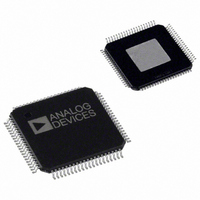
AD8384ASVZ Analog Devices Inc, AD8384ASVZ Datasheet - Page 8

AD8384ASVZ
Manufacturer Part Number
AD8384ASVZ
Description
IC DRIVER LCD 6CH 10BIT 80-TQFP
Manufacturer
Analog Devices Inc
Series
DecDriver™r
Datasheet
1.AD8384ASVZ.pdf
(24 pages)
Specifications of AD8384ASVZ
Display Type
LCD
Interface
3-Wire Serial
Current - Supply
40mA
Voltage - Supply
9 V ~ 18 V
Operating Temperature
0°C ~ 85°C
Mounting Type
Surface Mount
Package / Case
80-TQFP Exposed Pad, 80-eTQFP, 80-HTQFP, 80-VQFP
Lead Free Status / RoHS Status
Lead free / RoHS Compliant
Configuration
-
Digits Or Characters
-
Available stocks
Company
Part Number
Manufacturer
Quantity
Price
Company:
Part Number:
AD8384ASVZ
Manufacturer:
Analog Devices Inc
Quantity:
10 000
AD8384
ABSOLUTE MAXIMUM RATINGS
Table 6. AD8384 Stress Ratings
Parameter
Supply Voltages
Input Voltages
Internal Power Dissipation
Operating Temperature Range
Storage Temperature Range
Lead Temperature Range (Soldering 10 sec)
9
10
OVERLOAD PROTECTION
The AD8384 employs a 2-stage overload protection circuit that
consists of an output current limiter and a thermal shutdown.
The maximum current at any one output of the AD8384 is, on
average, internally limited to 100 mA. In the event of a momen-
tary short circuit between a video output and a power supply
rail (VCC or AGND), the output current limit is sufficiently low
to provide temporary protection.
The thermal shutdown debiases the output amplifier when the
junction temperature reaches the internally set trip point. In the
event of an extended short-circuit between a video output and a
power supply rail, the output amplifier current continues to
switch between 0 mA and 100 mA typical with a period deter-
mined by the thermal time constant and the hysteresis of the
thermal trip point. Thermal shutdown provides long term pro-
tection by limiting average junction temperature to a safe level.
EXPOSED PADDLE
To ensure optimized thermal performance, the exposed paddle
must be thermally connected to an external plane, such as
AVCC or GND, as described in the Application Notes.
Stresses above those listed under the Absolute Maximum Ratings may cause
permanent damage to the device. This is a stress rating only; functional
operation of the device at these or any other conditions above those
indicated in the operational section of this specification is not implied.
Exposure to the absolute maximum ratings for extended periods may
reduce device reliability.
θ
θ
80-lead TQFP E-pad package:
JA
JC
AVCCx – AGNDx
DVCC – DGND
Maximum Digital Input Voltage
Minimum Digital Input Voltage
Maximum Analog Input Voltage
Minimum Analog Input Voltages
TQFP E-Pad Package @ T
= 24°C/W (JEDEC STD, 4-layer PCB in still air)
= 16°C/W
10
A
= 25°C
9
Rating
18 V
4.5 V
DVCC + 0.5 V
DGND – 0.5 V
AVCC + 0.5 V
AGND – 0.5 V
4.16 W
0°C to 85°C
–65°C to +125°C
300°C
Rev. 0 | Page 8 of 24
MAXIMUM POWER DISSIPATION
The maximum power that can be safely dissipated by the
AD8384 is limited by its junction temperature. The maximum
safe junction temperature for plastic encapsulated devices, as
determined by the glass transition temperature of the plastic, is
approximately 150°C. Exceeding this limit temporarily may
cause a shift in the parametric performance due to a change in
the stresses exerted on the die by the package. Exceeding a
junction temperature of 175°C for an extended period can
result in device failure.
OPERATING TEMPERATURE RANGE
Although the maximum safe operating junction temperature is
higher, the AD8384 is 100% tested at a junction temperature of
125°C. Consequently, the maximum guaranteed operating
junction temperature is 125°C.
To ensure operation within the specified temperature range, it is
necessary to limit the maximum power dissipation as follows:
*AD8384 on a 4-layer JEDEC PCB with thermally optimized landing pattern, as
Note: When operating under the conditions specified in this
data sheet, the AD8384’s quiescent power dissipation is 1.1 W.
When driving a 6-channel XGA panel with a 150 pF input
capacitance, the AD8384 dissipates a total of 1.58 W when
displaying 1-pixel-wide alternating white and black vertical
lines generated by a standard 60 Hz XGA input video. When the
pixel clock frequency is raised to 100 MHz (the AD8384’s
maximum specified operating frequency), total power
dissipation increases to 1.83 W. Figure 2 shows these specific
power dissipations.
described in the Application Notes.
2.5
2.0
1.5
1.0
65
Figure 2. Maximum Power Dissipation vs. Temperature*
100MHz
60Hz XGA
QUIESCENT
70
P
DMAX
75
AMBIENT TEMPERATURE (°C)
≈
θ
200lfm
80
JA
–
0
500lfm
5 .
(
85
T
×
STILL AIR
JMAX
Airflow
–
90
T
A
)
(
95
lfm
)
100
105


