ISL6884IAZ Intersil, ISL6884IAZ Datasheet - Page 6
ISL6884IAZ
Manufacturer Part Number
ISL6884IAZ
Description
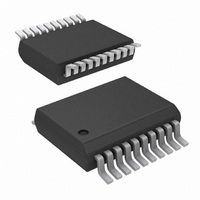
IC CTRLR CCFL BRIGHTNESS 20-SSOP
Manufacturer
Intersil
Datasheet
1.ISL6884IAZ.pdf
(13 pages)
Specifications of ISL6884IAZ
Display Type
CCFL - Cold Cathode Fluorescent Lamp
Interface
I²C
Voltage - Supply
4.5 V ~ 5.5 V
Operating Temperature
-40°C ~ 85°C
Mounting Type
Surface Mount
Package / Case
20-SSOP
Lead Free Status / RoHS Status
Lead free / RoHS Compliant
Current - Supply
-
Configuration
-
Digits Or Characters
-
Available stocks
Company
Part Number
Manufacturer
Quantity
Price
Company:

Part Number:
ISL6884IAZ
Manufacturer:
Intersil
Quantity:
480


Pin Description
VDD - Power input for digital systems. All functions are
disabled unless this pin exceeds 3V (see Power On Reset
specs). A 0.01µF decoupling cap should be placed between
VDD and GND with the shortest possible traces.
GND - Ground for digital systems.
REGCAP - An external 1µF capacitor to decouple the
internal 2.5V regulator.
EN - Logic level input signal. Voltage at this pin above a
threshold ENables circuit operation.
DPWM SYNC - A logic level input signal. The dimming PWM
frequency oscillator will synchronize to this signal (if
present). If no signal is present at this pin, the internal
DPWM oscillator will free run at approximately 160Hz.
PLL1 - Analog input. An RC network on these pins sets the
loop response of the DPWM Phase Locked Loop. A voltage
source or resister divider at this pin will set the DPWM
frequency. See the graph below for approximate frequency
vs voltage at PLL1.
Electrical Specifications
NOTE:
DPWM
DPWM PLL Free Run Frequency
DPWM PLL Lock Frequency
Lock Time
DPWM Duty Cycle
DPWM Duty Cycle
DPWM Duty Cycle
DPWM Output High
DPWM Output Low
DPWM Rise Time
DPWM Fall Time
2. Master enable (0X2B) = 01, channel enable (0X2C) = FF, all other registers in default mode
220
200
180
160
140
120
100
PARAMETER
80
60
0.5
Voltage at PLL1 (V)
0.7
6
F_DPWM=V_PLL1*160+8
measured
Recommended Operating Conditions, Unless Otherwise Noted (Continued)
0.9
DPWM
DPWM
DPWM
T
T
SYMBOL
rise_DPWM
fall_DPWM
f
freerun
T
V
f
V
lock
lock
OH
1.1
OL
DCmax
DCmin
DCmid
BRT_M = 00hex (Note 3)
BRT_M = 7Fhex (Note 3)
BRT_M = FFhex (Note 3)
I
I
Cload = 200pF
Cload = 200pF
OH
OL
1.3
= 2mA
= 2mA
ISL6884
TEST CONDITIONS
GNDPLL - A separate ground terminal for the PLL. Filter
and bias components on PLL1 should be connected to this
ground with the shortest possible traces. This pin is also
connected to the system ground with a trace that is not
critical.
DPWM 1:8 - Logic level outputs that control the analog and
PWM dimming of each of 8 ISL6882s. The duty cycle of the
DPWM signals range from 4% (minimum brightness) to
100% (maximum brightness). A low pass filter in the inverter
Controller converts the DPWM duty cycle to a DC voltage
that performs 3:1 analog dimming. The combined dimming
range is 100:1. The dimming value is set by I
LAMP_ON - A logic level input signal. A high level on the pin
indicates that all lamps are ON and operating normally. A low
level at this pin indicates that at least one of the lamps is
either not ignited or out of the circuit. When this pin is low,
the fault timer runs. When this pin is high, the fault timer is
reset. Because this is a high impedance line that may be
routed near sources of EMI, it is recommended that a 10K
resister is placed in series between the LAMP_ON pin and
all other circuits.
SDA, SCL - Logic level input/output signals. SDA is the I
data line and SCL is the I
receives data via I
dimming for each channel, and set the number of channels.
System status can be read via I
TESTEN and OSCTEST - These pins are used for internal
tests. They should be left unconnected in normal operation.
2
C to enable or disable the inverters, set
0.7*VDD
MIN
120
49
98
3
-
-
-
-
-
2
C clock line. The ISL6884
2
C.
TYP
160
160
150
50
4
-
-
-
-
-
0.3*VDD
MAX
200
100
500
500
51
2
5
-
-
-
C registers.
March 9, 2006
UNITS
FN9265.0
ms
Hz
Hz
ns
ns
%
%
%
V
V
2
C
Related parts for ISL6884IAZ
Image
Part Number
Description
Manufacturer
Datasheet
Request
R

Part Number:
Description:
CCFL Brightness Controller
Manufacturer:
Intersil Corporation
Datasheet:
Part Number:
Description:
Intersil Corporation [CMOS Serial Controller Interface]
Manufacturer:
Intersil Corporation
Datasheet:
Part Number:
Description:
Manufacturer:
Intersil Corporation
Datasheet:
Part Number:
Description:
357-036-542-201 CARDEDGE 36POS DL .156 BLK LOPRO
Manufacturer:
Intersil Corporation
Datasheet:
Part Number:
Description:
1024-Word x 4-Bit LSI Static RAM
Manufacturer:
Intersil Corporation
Datasheet:
Part Number:
Description:
General Purpose NPN Transistor Arrays FN341.4
Manufacturer:
Intersil Corporation
Datasheet:
Part Number:
Description:
CMOS 16-Bit Microprocessor
Manufacturer:
Intersil Corporation
Datasheet:
Part Number:
Description:
Manufacturer:
Intersil Corporation
Datasheet:
Part Number:
Description:
Manufacturer:
Intersil Corporation
Datasheet:
Part Number:
Description:
Manufacturer:
Intersil Corporation
Datasheet:
Part Number:
Description:
Manufacturer:
Intersil Corporation
Datasheet:
Part Number:
Description:
CMOS 6-Bit Latch and Decoder Memory Interfaces
Manufacturer:
Intersil Corporation
Datasheet:
Part Number:
Description:
CA3046General Purpose NPN Transistor Arrays
Manufacturer:
Intersil Corporation
Datasheet:
Part Number:
Description:
Manufacturer:
Intersil Corporation
Datasheet:
Part Number:
Description:
TR909 DLC/FLC SLIC with Low Power Standby
Manufacturer:
Intersil Corporation
Datasheet: