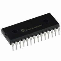
TC7135CPI Microchip Technology, TC7135CPI Datasheet - Page 7

TC7135CPI
Manufacturer Part Number
TC7135CPI
Description
IC ADC 4 1/2DGT 28-DIP
Manufacturer
Microchip Technology
Datasheet
1.TC7135CPI.pdf
(28 pages)
Specifications of TC7135CPI
Display Type
LED
Configuration
7 Segment
Interface
BCD
Digits Or Characters
A/D 4.5 Digits
Current - Supply
1mA
Voltage - Supply
4 V ~ 6 V
Operating Temperature
0°C ~ 70°C
Mounting Type
Through Hole
Package / Case
28-DIP (0.600", 15.24mm)
Lead Free Status / RoHS Status
Lead free / RoHS Compliant
Other names
158-1133
158-1133
TC7135CPIR
TC7135CPIR
158-1133
TC7135CPIR
TC7135CPIR
Available stocks
Company
Part Number
Manufacturer
Quantity
Price
Company:
Part Number:
TC7135CPI
Manufacturer:
MICROCHIP
Quantity:
12 000
Part Number:
TC7135CPI
Manufacturer:
MICROCHIP/微芯
Quantity:
20 000
3.2.1
During this phase, errors due to buffer, integrator and
comparator offset voltages are compensated for by
charging C
ing error voltage. With a zero input voltage, the
integrator output will remain at zero.
The external input signal is disconnected from the
internal circuitry by opening the two SW
internal input points connect to the ANALOG
COMMON pin. The reference capacitor charges to the
reference voltage potential through SW
loop, closed around the integrator and comparator,
charges the C
sate for buffer amplifier, integrator and comparator
offset voltages (see
FIGURE 3-2:
3.2.2
The TC7135 integrates the differential voltage between
the +INPUT and -INPUT pins. The differential voltage
must be within the device Common mode range; -1V
from either supply rail, typically. The input signal
polarity is determined at the end of this phase.
FIGURE 3-3:
Phase.
© 2007 Microchip Technology Inc.
Analog
Common
Analog
Common
REF
REF
+IN
+IN
IN
IN
IN
IN
SW
SW
SW
SW
SW
SW
SW
SW
Z
Z
R
R
I
I
I
I
AZ
SYSTEM ZERO
ANALOG INPUT SIGNAL
INTEGRATION
(auto-zero capacitor) with a compensat-
AZ
C
C
REF
REF
capacitor with a voltage to compen-
SW
SW
Input Buffer
Input Buffer
Figure
Analog
1
1
Analog
SW
SW
System Zero Phase.
Input Signal Integration
+
–
SW
+
–
SW
IZ
IZ
Z
Z
3-2).
SW
SW
R
R
INT
Z
INT
Z
Integrator
Integrator
C
C
C
C
+
–
–
+
SZ
SZ
INT
Switch Open
Switch Closed
INT
Switch Open
Switch Closed
I
R
switches. The
. A feedback
+
–
+
–
Comparator
Comparator
To
Digital
Section
To
Digital
Section
3.2.3
The previously charged reference capacitor is con-
nected with the proper polarity to ramp the integrator
output back to zero
reading displayed is:
EQUATION 3-3:
FIGURE 3-4:
Integration Cycle.
3.2.4
This phase ensures the integrator output is at 0V when
the system zero phase is entered. It also ensures that
the true system offset voltages are compensated for.
This phase normally lasts 100 to 200 clock cycles. If an
overrange condition exists, the phase is extended to
6200 clock cycles (see
FIGURE 3-5:
Phase.
Analog
Common
Analog
Common
REF
REF
+IN
+IN
IN
IN
IN
IN
SW
SW
SW
SW
SW
SW
SW
SW
Z
Z
Reading
R
R
I
I
I
I
REFERENCE VOLTAGE
INTEGRATION
INTEGRATOR OUTPUT ZERO
C
C
REF
REF
=
SW
SW
10 000
Input Buffer
Input Buffer
1
1
Analog
SW
Analog
,
Reference Voltage
SW
Integrator Output Zero
+
–
SW
+
–
SW
Figure
(
see
IZ
IZ
Z
Z
[
---------------------------------------------- -
SW
SW
Differential Input
R
Figure
R
3-5).
INT
Z
INT
Z
V
Integrator
Integrator
TC7135
REF
C
C
C
C
+
–
+
SZ
–
SZ
3-4). The digital
INT
INT
Switch Open
Switch Closed
Switch Closed
Switch Open
DS21460D-page 7
+
–
+
–
Comparator
Comparator
]
To
Digital
Section
To
Digital
Section


