ADE7753ARSZ Analog Devices Inc, ADE7753ARSZ Datasheet - Page 19

ADE7753ARSZ
Manufacturer Part Number
ADE7753ARSZ
Description
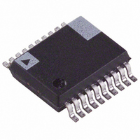
IC ENERGY METERING 1PHASE 20SSOP
Manufacturer
Analog Devices Inc
Datasheet
1.ADE7753ARSZ.pdf
(60 pages)
Specifications of ADE7753ARSZ
Input Impedance
390 KOhm
Measurement Error
0.1%
Voltage - I/o High
2.4V
Voltage - I/o Low
0.8V
Current - Supply
3mA
Voltage - Supply
4.75 V ~ 5.25 V
Operating Temperature
-40°C ~ 85°C
Mounting Type
Surface Mount
Package / Case
20-SSOP (0.200", 5.30mm Width)
Meter Type
Single Phase
Ic Function
Single-Phase Multifunction Metering IC
Supply Voltage Range
4.75V To 5.25V
Operating Temperature Range
-40°C To +85°C
Digital Ic Case Style
SSOP
No. Of Pins
20
Lead Free Status / RoHS Status
Lead free / RoHS Compliant
For Use With
EVAL-ADE7753ZEB - BOARD EVALUATION AD7753
Lead Free Status / RoHS Status
Lead free / RoHS Compliant, Lead free / RoHS Compliant
Available stocks
Company
Part Number
Manufacturer
Quantity
Price
Part Number:
ADE7753ARSZ
Manufacturer:
ADI/亚德诺
Quantity:
20 000
Part Number:
ADE7753ARSZRL
Manufacturer:
ADI/亚德诺
Quantity:
20 000
FULL SCALE
SAGLVL [7:0]
Figure 43 shows the line voltage falling below a threshold that is
set in the sag level register (SAGLVL[7:0]) for three line cycles.
The quantities 0 and 1 are not valid for the SAGCYC register,
and the contents represent one more than the desired number
of full line cycles. For example, when the sag cycle (SAGCYC[7:0])
contains 0x04, the SAG pin goes active low at the end of the
third line cycle for which the line voltage (Channel 2 signal)
falls below the threshold, if the DISSAG bit in the mode register
is Logic 0. As is the case when zero crossings are no longer
detected, the sag event is also recorded by setting the SAG flag
in the interrupt status register. If the SAG enable bit is set to
Logic 1, the IRQ logic output goes active low—see the ADE7753
Interrupts section. The SAG pin goes logic high again when the
absolute value of the signal on Channel 2 exceeds the sag level
set in the sag level register. This is shown in Figure 43 when the
SAG pin goes high again during the fifth line cycle from the
time when the signal on Channel 2 first dropped below the
threshold level.
Sag Level Set
The contents of the sag level register (1 byte) are compared to
the absolute value of the most significant byte output from LPF1
after it is shifted left by one bit, thus, for example, the nominal
maximum code from LPF1 with a full-scale signal on Channel 2
is 0x2518—see the Channel 2 Sampling section. Shifting one bit
left gives 0x4A30. Therefore writing 0x4A to the SAG level
register puts the sag detection level at full scale. Writing 0x00 or
0x01 puts the sag detection level at 0. The SAG level register is
compared to the most significant byte of a waveform sample
after the shift left and detection is made when the contents of
the sag level register are greater.
PEAK DETECTION
The ADE7753 can also be programmed to detect when the
absolute value of the voltage or current channel exceeds a
specified peak value. Figure 44 illustrates the behavior of the
peak detection for the voltage channel. Both Channel 1 and
Channel 2 are monitored at the same time.
SAG
SAGCYC [7:0] = 0x04
Figure 43. ADE7753 Sag Detection
3 LINE CYCLES
CHANNEL 2
SAG RESET HIGH
WHEN CHANNEL 2
EXCEEDS SAGLVL [7:0]
02875-0-043
Rev. A | Page 19 of 60
STATUS REGISTER)
Figure 44 shows a line voltage exceeding a threshold that is set
in the voltage peak register (VPKLVL[7:0]). The voltage peak
event is recorded by setting the PKV flag in the interrupt status
register. If the PKV enable bit is set to Logic 1 in the interrupt
mask register, the IRQ logic output goes active low. Similarly, the
current peak event is recorded by setting the PKI flag in the
interrupt status register—see the ADE7753 Interrupts section.
Peak Level Set
The contents of the VPKLVL and IPKLVL registers are
respectively compared to the absolute value of Channel 1 and
Channel 2 after they are multiplied by 2. Thus, for example, the
nominal maximum code from the Channel 1 ADC with a full-
scale signal is 0x2851EC—see the Channel 1 Sampling section.
Multiplying by 2 gives 0x50A3D8. Therefore, writing 0x50 to
the IPKLVL register, for example, puts the Channel 1 peak
detection level at full scale and sets the current peak detection
to its least sensitive value. Writing 0x00 puts the Channel 1
detection level at 0. The detection is done by comparing the
contents of the IPKLVL register to the incoming Channel 1
sample. The IRQ pin indicates that the peak level is exceeded if
the PKI or PKV bits are set in the interrupt enable register
(IRQEN[15:0]) at Address 0x0A.
Peak Level Record
The ADE7753 records the maximum absolute value reached by
Channel 1 and Channel 2 in two different registers—IPEAK
and VPEAK, respectively. VPEAK and IPEAK are 24-bit unsigned
registers. These registers are updated each time the absolute
value of the waveform sample from the corresponding channel
is above the value stored in the VPEAK or IPEAK register. The
contents of the VPEAK register correspond to 2× the maximum
absolute value observed on the Channel 2 input. The contents of
IPEAK represent the maximum absolute value observed on the
Channel 1 input. Reading the RSTVPEAK and RSTIPEAK
registers clears their respective contents after the read operation.
READ RSTSTATUS
PKV INTERRUPT
FLAG (BIT 8 OF
VPKLVL[7:0]
REGISTER
V
2
Figure 44. ADE7753 Peak Level Detection
PKV RESET LOW
WHEN RSTSTATUS
REGISTER IS READ
ADE7753
02875-0-088


