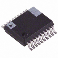
ADE7753ARSZ Analog Devices Inc, ADE7753ARSZ Datasheet - Page 49

ADE7753ARSZ
Manufacturer Part Number
ADE7753ARSZ
Description
IC ENERGY METERING 1PHASE 20SSOP
Manufacturer
Analog Devices Inc
Datasheet
1.ADE7753ARSZ.pdf
(60 pages)
Specifications of ADE7753ARSZ
Input Impedance
390 KOhm
Measurement Error
0.1%
Voltage - I/o High
2.4V
Voltage - I/o Low
0.8V
Current - Supply
3mA
Voltage - Supply
4.75 V ~ 5.25 V
Operating Temperature
-40°C ~ 85°C
Mounting Type
Surface Mount
Package / Case
20-SSOP (0.200", 5.30mm Width)
Meter Type
Single Phase
Ic Function
Single-Phase Multifunction Metering IC
Supply Voltage Range
4.75V To 5.25V
Operating Temperature Range
-40°C To +85°C
Digital Ic Case Style
SSOP
No. Of Pins
20
Lead Free Status / RoHS Status
Lead free / RoHS Compliant
For Use With
EVAL-ADE7753ZEB - BOARD EVALUATION AD7753
Lead Free Status / RoHS Status
Lead free / RoHS Compliant, Lead free / RoHS Compliant
Available stocks
Company
Part Number
Manufacturer
Quantity
Price
Part Number:
ADE7753ARSZ
Manufacturer:
ADI/亚德诺
Quantity:
20 000
Part Number:
ADE7753ARSZRL
Manufacturer:
ADI/亚德诺
Quantity:
20 000
ADE7753 Serial Write Operation
The serial write sequence takes place as follows. With the
ADE7753 in communications mode (i.e., the CS input logic
low), a write to the communications register first takes place.
The MSB of this byte transfer is a 1, indicating that the data
transfer operation is a write. The LSBs of this byte contain the
address of the register to be written to. The ADE7753 starts
shifting in the register data on the next falling edge of SCL
remaining bits of register data are shifted in on the falling edge
of subsequent SCLK pulses—see Figure 92. As explained earlie
the data write is initiated by a write to the communications
register followed by the data. During a data write operation to
the ADE7753, data is transferred to all on-chip registers one
byte at a time. After a byte is transferred into the serial port,
there is a finite time before it is transferred to one of the
ADE7753 on-chip registers. Although another byte transfer to
the serial port can start while the previous byte is being
transferred to an on-chip register, this second byte transfer
SCLK
DIN
CS
SCLK
DIN
t
1
1
X
0
t
2
A5
X
t
3
COMMAND BYTE
A4
MOST SIGNIFICANT BYTE
X
t
4
A3
X
t
5
A2
DB11 DB10
Figure 93. 12-Bit Serial Write Operation
Figure 92. Serial Interfac
A1
K. All
A0
Rev. A | Page 49 of 60
DB9
r,
t
7
DB8
D
e Write Timing
B7
DB7
should not finish until at least 4 µs after the end of the previous
byte transfer. This functionality is expressed in the timing
specification t
during a byte transfer ( CS brought high), then that byte cannot
be written to the destination register.
Destination registers can be up to 3 bytes wide—see the
ADE
shifted into the serial port at DI is transferred to the MSB
(most significant byte) of the destination register. If, for
example, the addressed register is 12 bits wide, a 2-byte data
transfer must take place. The data is always assumed to be right
justified, therefore in this case, the four MSBs of the first byte
would be ignored and the four LSBs of the first byte written to
the A
Figure 93 illustrates this example.
MOST SIGNIFICANT BYTE
7753 Register Description tables. Therefore the first byte
DE7753 would be the four MSBs of the 12-bit word.
DB6
DB5
LEAST SIGNIFICANT BYTE
6
—see Figure 92. If a write operation is aborted
DB4
DB0
DB3
t
7
DB2
LEAST SIGNIFICANT BYTE
DB7
N
DB1
t
6
DB0
02875-0-082
DB0
t
ADE7753
8
02875-0-081


