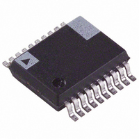
ADE7763ARSZRL Analog Devices Inc, ADE7763ARSZRL Datasheet - Page 19

ADE7763ARSZRL
Manufacturer Part Number
ADE7763ARSZRL
Description
IC ENERGY METERING 1PHASE 20SSOP
Manufacturer
Analog Devices Inc
Datasheet
1.ADE7763ARSZRL.pdf
(56 pages)
Specifications of ADE7763ARSZRL
Input Impedance
390 KOhm
Measurement Error
0.1%
Voltage - I/o High
2.4V
Voltage - I/o Low
0.8V
Current - Supply
3mA
Voltage - Supply
4.75 V ~ 5.25 V
Operating Temperature
-40°C ~ 85°C
Mounting Type
Surface Mount
Package / Case
20-SSOP (0.200", 5.30mm Width)
Meter Type
Single Phase
Ic Function
Single-Phase Active And Apparent Energy Metering IC
Supply Voltage Range
4.75V To 5.25V
Operating Temperature Range
-40°C To +85°C
Digital Ic Case Style
SSOP
No. Of Pins
20
Lead Free Status / RoHS Status
Lead free / RoHS Compliant
For Use With
EVAL-ADE7763ZEB - BOARD EVALUATION FOR ADE7763
Lead Free Status / Rohs Status
Compliant
Other names
ADE7763ARSZRL
ADE7763ARSZRLTR
ADE7763ARSZRLTR
Available stocks
Company
Part Number
Manufacturer
Quantity
Price
Part Number:
ADE7763ARSZRL
Manufacturer:
ADI/亚德诺
Quantity:
20 000
LOW-PASS FILTER
Interrupt Timing
Review the Serial Interface section before reading this section.
As previously described, when the IRQ output goes low, the
MCU ISR will read the interrupt status register to determine the
source of the interrupt. When reading the status register
contents, the IRQ output is set high upon the last falling edge of
SCLK of the first byte transfer (read interrupt status register
command). The IRQ output is held high until the last bit of the
next 15-bit transfer is shifted out (interrupt status register
contents)—see
the
IRQ output will stay high.
TEMPERATURE MEASUREMENT
There is an on-chip temperature sensor. A temperature
measurement can be made by setting Bit 5 in the mode register.
When Bit 5 is set logic high in the mode register, the ADE7763
initiates a temperature measurement of the next zero crossing.
When the zero crossing on Channel 2 is detected, the voltage
output from the temperature sensing circuit is connected to
ADC1 (Channel 1) for digitizing. The resulting code is
processed and placed in the temperature register (TEMP[7:0])
approximately 26 μs later (24 CLKIN/4 cycles). If enabled in the
interrupt enable register (Bit 5), the IRQ output will go active
low when the temperature conversion is finished.
The contents of the temperature register are signed (twos
complement) with a resolution of approximately 1.5 LSB/°C.
The temperature register produces a code of 0x00 when the
ambient temperature is approximately −25°C. The temperature
measurement is uncalibrated in the ADE7763 and might have
an offset tolerance as high as ±25°C.
ANALOG-TO-DIGITAL CONVERSION
The analog-to-digital conversion is carried out using two
second-order Σ -Δ ADCs. For simplicity, the block diagram in
Figure 39 shows a first-order Σ -Δ ADC. The converter
comprises two parts: the Σ -Δ modulator and the digital low-
pass filter.
A Σ -Δ modulator converts the input signal into a continuous
serial stream of 1s and 0s at a rate determined by the sampling
clock. In the ADE7763, the sampling clock is equal to CLKIN/4.
The 1-bit DAC in the feedback loop is driven by the serial data
ANALOG
IRQ output will go low again. If no interrupt is pending, the
R
C
Figure 37
+
Figure 39. First-Order
–
INTEGRATOR
. If an interrupt is pending at this time,
V
REF
1-BIT DAC
.....10100101.....
MCLK/4
+
–
LATCHED
COMPARATOR
Σ
-Δ ADC
LOW-PASS
DIGITAL
FILTER
24
Rev. B | Page 19 of 56
stream. The DAC output is subtracted from the input signal. If
the loop gain is high enough, the average value of the DAC
output (and therefore the bit stream) will approach that of the
input signal level. For any given input value in a single sampling
interval, the data from the 1-bit ADC is virtually meaningless.
Only when a large number of samples are averaged can a
meaningful result be obtained. This averaging is carried out in
the second part of the ADC, the digital low-pass filter. By
averaging a large number of bits from the modulator, the low-
pass filter can produce 24-bit data-words that are proportional
to the input signal level.
The Σ -Δ converter uses two techniques to achieve high resolution
from what is essentially a 1-bit conversion technique. The first
is oversampling. Oversampling means that the signal is sampled
at a rate (frequency) that is many times higher than the band-
width of interest. For example, the sampling rate in the ADE7763
is CLKIN/4 (894 kHz) and the band of interest is 40 Hz to 2 kHz.
Oversampling has the effect of spreading the quantization noise
(noise due to sampling) over a wider bandwidth. With the noise
spread more thinly over a wider bandwidth, the quantization
noise in the band of interest decreases—see Figure 40. However,
oversampling alone is not efficient enough to improve the
signal-to-noise ratio (SNR) in the band of interest. For example,
an oversampling ratio of 4 is required just to increase the SNR
by 6 dB (1 bit). To keep the oversampling ratio at a reasonable
level, it is possible to shape the quantization noise so that the
majority of the noise lies at higher frequencies. In the Σ -Δ
modulator, the noise is shaped by the integrator, which has a
high-pass-type response for the quantization noise. The result is
that most of the noise is at higher frequencies, where it can
be removed by the digital low-pass filter. This noise shaping is
shown in Figure 40.
SIGNAL
SIGNAL
NOISE
NOISE
0
0
Figure 40. Noise Reduction due to Oversampling and
OUTPUT FROM DIGITAL
Noise Shaping in the Analog Modulator
2
2
HIGH RESOLUTION
DIGITAL
FILTER
LPF
FREQUENCY (kHz)
FREQUENCY (kHz)
FILTER (RC)
ANTIALIAS
447
447
SHAPED
NOISE
FREQUENCY
SAMPLING
ADE7763
894
894


