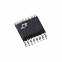
LT4254IGN Linear Technology, LT4254IGN Datasheet - Page 11

LT4254IGN
Manufacturer Part Number
LT4254IGN
Description
IC CTLR HOTSWAP POS 16-SSOP
Manufacturer
Linear Technology
Type
Hot-Swap Controllerr
Datasheet
1.LT4254CGNPBF.pdf
(16 pages)
Specifications of LT4254IGN
Applications
General Purpose
Internal Switch(s)
No
Voltage - Supply
10.8 V ~ 36 V
Operating Temperature
-40°C ~ 85°C
Mounting Type
Surface Mount
Package / Case
16-SSOP (0.150", 3.90mm Width)
Lead Free Status / RoHS Status
Contains lead / RoHS non-compliant
Available stocks
Company
Part Number
Manufacturer
Quantity
Price
Company:
Part Number:
LT4254IGN
Manufacturer:
LT
Quantity:
10 000
Part Number:
LT4254IGN
Manufacturer:
LINEAR/凌特
Quantity:
20 000
Part Number:
LT4254IGN#PBF
Manufacturer:
LINEAR/凌特
Quantity:
20 000
Part Number:
LT4254IGN#TRPBF
Manufacturer:
LINEAR/凌特
Quantity:
20 000
APPLICATIO S I FOR ATIO
Layout Considerations section for important information
about board layout to minimize current limit threshold
error.
The LT4254 also features a variable overcurrent response
time. The time required for the part to regulate the GATE
pin voltage is a function of the voltage across the sense
resistor connected between the V
This helps to eliminate sensitivity to current spikes and tran-
sients that might otherwise unnecessarily trigger a current
limit response and increase MOSFET dissipation. Figure 8
shows the response time as a function of the overdrive at
the SENSE pin.
TIMER
The TIMER pin provides a method for programming the
maximum time the part is allowed to operate in current
limit. When the current limit circuitry is not active, the
TIMER pin is pulled to GND by a 3µA current source. When
the current limit circuitry becomes active, a 123µA pull-up
current source is added to the TIMER pin and the voltage
will rise with a slope equal to 120µA/C
circuitry stays active. Once the desired maximum current
limit time is known, the capacitor value is:
Whenever the TIMER pin reaches 4.65V (typ), the internal
fault latch is set causing the GATE to be pulled low and the
TIMER pin to be discharged to GND by the 3µA current
source. The part is not allowed to turn on again until the
voltage at the TIMER pin falls below 0.65V (typ).
Figure 7. Current Limit Sense Voltage vs Feedback Pin Voltage
C(nF) = 25.8 • t(ms)
V
CC
– V
SENSE
50mV
12mV
0V
U
U
2V
CC
pin and the SENSE pin.
W
TIMER
as long as the
4254
FB
U
F07
The TIMER pin must never be pulled high by a low
impedance because whenever the TIMER pin voltage rises
above the upper threshold (typically 4.65V) the pin char-
acteristics change from a high impedance current source
to a low impedance. If the pin must be pulled high by a logic
signal, then a resistor must be put in series with the TIMER
pin to limit the current to approximately 100 microam-
peres. The resistance should be chosen as follows:
Whenever the GATE pin is commanded off by any fault
condition, it is discharged with a high current, turning off
the external MOSFET. The waveform in Figure 9 shows how
the output latches off following a short-circuit. The drop
across the sense resistor is held at 12mV as the timer ramps
up. Since the output did not rise bringing FB above 2V and
the current is still 12mV/R5, the circuit latches off.
Automatic Restart
If the RETRY pin is floating, then the functionality is as
described in the previous section.
When the voltage at the TIMER pin ramps back down to
0.65V (typ), the LT4254 turns on again. If the short-circuit
condition at the output still exists, the cycle will repeat
itself indefinitely. The duty cycle under short-circuit con-
ditions is 3% which prevents Q1 from overheating.
Latch Off Operation
If the RETRY pin is grounded, the LT4254 will latch off
after a current fault. After the part latches off, it may be
R
SERIES
12
10
8
6
4
2
0
Figure 8. Response Time to Overcurrent
= (V
LOGIC
50
– 4.65V)/100µA
V
100
CC
– V
SENSE
(mV)
150
LT4254
200
11
4254 F08
4254fb


