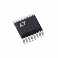
LT4254IGN Linear Technology, LT4254IGN Datasheet - Page 12

LT4254IGN
Manufacturer Part Number
LT4254IGN
Description
IC CTLR HOTSWAP POS 16-SSOP
Manufacturer
Linear Technology
Type
Hot-Swap Controllerr
Datasheet
1.LT4254CGNPBF.pdf
(16 pages)
Specifications of LT4254IGN
Applications
General Purpose
Internal Switch(s)
No
Voltage - Supply
10.8 V ~ 36 V
Operating Temperature
-40°C ~ 85°C
Mounting Type
Surface Mount
Package / Case
16-SSOP (0.150", 3.90mm Width)
Lead Free Status / RoHS Status
Contains lead / RoHS non-compliant
Available stocks
Company
Part Number
Manufacturer
Quantity
Price
Company:
Part Number:
LT4254IGN
Manufacturer:
LT
Quantity:
10 000
Part Number:
LT4254IGN
Manufacturer:
LINEAR/凌特
Quantity:
20 000
Part Number:
LT4254IGN#PBF
Manufacturer:
LINEAR/凌特
Quantity:
20 000
Part Number:
LT4254IGN#TRPBF
Manufacturer:
LINEAR/凌特
Quantity:
20 000
APPLICATIO S I FOR ATIO
LT4254
commanded to start back up. This can be commanded by
cycling the UV pin to ground and then back high (this
command can only be accepted after the TIMER pin
discharges below the 0.65V typ threshold, so as to prevent
overheating transistor Q1).
Therefore, using the RETRY pin only, the LT4254 will
either latch off after an overcurrent fault condition or it will
go into a hiccup mode.
Undervoltage and Overvoltage Detection
The LT4254 uses the UV and OV pins to monitor the V
voltage and allow the user the greatest flexibility for setting
the operational thresholds. The UV and OV pins are
internally connected to an analog window comparator.
Any time that the UV pin goes below 3.6V or the OV pin
goes above 4V, the gate will be pulled low until the UV/OV
pin voltages return to the normal operation voltage win-
dow (4V and 3.65V, respectively).
Power Good Detection
The LT4254 includes a comparator for monitoring the
output voltage. The output voltage is sensed through the
FB pin via an external resistor string. The comparator’s
output (PWRGD pin) is an open collector capable of
operating from a pull-up as high as 36V.
The PWRGD pin can be used to directly enable/disable a
power module with an active high enable input. Figure 11
shows how to use the PWRGD pin to control an active low
enable input power module. Signal inversion is accom-
plished by transistor Q2 and R10.
12
500mA/DIV
20V/DIV
20V/DIV
5V/DIV
TIMER
GATE
V
I
OUT
OUT
Figure 9. Latch Off Waveforms
U
Latch Off Operation
2.5ms/DIV
U
W
4254 F09
U
CC
Open FET Detection
The LT4254 can be used to detect the presence of an open
FET. When the voltage across the sense resistor is less
than 3.5mV, the open collector pull-down device is shut
off allowing the OPEN pin to be externally pulled high.
An open FET condition is signalled when the OPEN pin is
high and the PWRGD pin is low (after the part has
completed its start-up cycle). This open FET condition can
be falsely signalled during start-up if the load is not
activated until after PWRGD goes high. To avoid this false
indication, the OPEN and PWRGD pins should not be
polled for a period of time, t
This can be accomplished either by a microcontroller (if
available) or by placing an RC filter as shown in Figure 12.
Once the OPEN voltage exceeds the monitoring logic thresh-
old, V
is signalled. In order to prevent a false indication, the RC
product should be set with the following equation:
Another condition that can cause a false indication is if the
LT4254 goes into current limit during start-up. This will
cause t
500mA/DIV
RC
3
20V/DIV
•
5V/DIV
1V/DIV
TIMER
THRESH
35
GATE
V
V
>
Automatic Restart Operation (Short-Ciruit Output)
I
STARTUP
OUT
OUT
CC
µ
35
A
•
µ
C
, and PWRGD is low, an open FET condition
A
1
⎛
⎜
⎝
=
Figure 10. RETRY Waveforms
ln
to be longer than calculated. Also, if the
t
⎛
⎜
⎝
STARTUP
3
V
LOGIC
•
V
CC
V
2.5ms/DIV
LOGIC
•
–
C
STARTUP
V
1
THRESH
, given by:
⎞
⎟
⎠
⎞
⎟
⎠
4254 F10
4254fb


