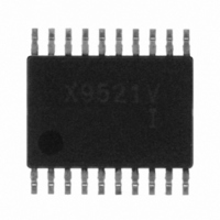
X9521V20I-A Intersil, X9521V20I-A Datasheet - Page 14

X9521V20I-A
Manufacturer Part Number
X9521V20I-A
Description
IC DCP DUAL EEPROM MEM 20-TSSOP
Manufacturer
Intersil
Type
Laser Diode Controller (Fiber Optic)r
Datasheet
1.X9521V20I.pdf
(24 pages)
Specifications of X9521V20I-A
Number Of Channels
2
Voltage - Supply
2.7 V ~ 5.5 V
Current - Supply
1.5mA
Operating Temperature
-40°C ~ 85°C
Package / Case
20-TSSOP
Mounting Type
Surface Mount
Lead Free Status / RoHS Status
Contains lead / RoHS non-compliant
Other names
X9521V20I-AIS
For example, a sequence of writes to the device CON-
STAT register consisting of [02H, 06H, 02H] will reset the
BL0 and BL0 bits in the CONSTAT Register to “0”.
It should be noted that a write to any nonvolatile bit of
CONSTAT register will be ignored if the Write Protect
pin of the X9521 is active (HIGH) (See "WP: Write Pro-
tection Pin").
CONSTAT Register Read Operation
The contents of the CONSTAT Register can be read at
any time by performing a random read (See Figure 19).
Using the Slave Address Byte set to 10100101, and an
Address Byte of FFh. Only one byte is read by each reg-
ister read operation. The X9521 resets itself after the first
byte is read. The master should supply a STOP condition
to be consistent with the bus protocol.
After setting the WEL and / or the RWEL bit(s) to a “1”,
a CONSTAT register read operation may occur, without
interrupting a proceeding CONSTAT register write
operation.
When reading the contents of the CONSTAT register,
the bits CS7 - CS5 and CS0 will always return “0”.
X9521 Write Permission Status
Block Lock
BL0
x
1
0
x
1
0
Bits
BL1
Signals from
the Master
Signals from
the Slave
1
x
0
1
x
0
SDA Bus
WP
0
0
0
1
1
1
DCP Volatile Write
Figure 19. CONSTAT Register Read Command Sequence
Permitted
14
YES
YES
S
a
r
NO
NO
NO
NO
t
t
1
0 1 0 0 1 0
Address
Slave
“Dummy” Write
0
DCP Nonvolatile
Write Permitted
A
C
K
WRITE Operation
YES
Address
NO
NO
NO
NO
NO
Byte
X9521
A
C
K
DATA PROTECTION
There are a number of levels of data protection features
designed into the X9521. Any write to the device first
requires setting of the WEL bit in the CONSTAT register.
A write to the CONSTAT register itself, further requires
the setting of the RWEL bit. Block Lock protection of the
device enables the user to inhibit writes to certain regions
of the EEPROM memory, as well as to all the DCPs. One
further level of data protection in the X9521, is incorpo-
rated in the form of the Write Protection pin.
WP: Write Protection Pin
When the Write Protection (WP) pin is active (HIGH), it
disables nonvolatile write operations to the X9521.
The table below (X9521 Write Permission Status) sum-
marizes the effect of the WP pin (and Block Lock), on the
write permission status of the device.
Additional Data Protection Features
In addition to the preceding features, the X9521 also
incorporates the following data protection functionality:
—The proper clock count and data bit sequence is
Not in locked region
Not in locked region
S
a
t
r
t
Write to EEPROM
1 0 1 0 0 1 0
required prior to the STOP bit in order to start a nonvol-
atile write cycle.
Yes (All Array)
Address
Permitted
Slave
NO
NO
NO
1
READ Operation
C
A
K
CS7 … CS0
Volatile Bits
Data
Write to CONSTAT Register
YES
YES
YES
NO
NO
NO
Permitted
S
o
p
t
Nonvolatile Bits
September 21, 2010
YES
YES
YES
NO
NO
NO
FN8207.2


