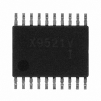
X9521V20I-A Intersil, X9521V20I-A Datasheet - Page 8

X9521V20I-A
Manufacturer Part Number
X9521V20I-A
Description
IC DCP DUAL EEPROM MEM 20-TSSOP
Manufacturer
Intersil
Type
Laser Diode Controller (Fiber Optic)r
Datasheet
1.X9521V20I.pdf
(24 pages)
Specifications of X9521V20I-A
Number Of Channels
2
Voltage - Supply
2.7 V ~ 5.5 V
Current - Supply
1.5mA
Operating Temperature
-40°C ~ 85°C
Package / Case
20-TSSOP
Mounting Type
Surface Mount
Lead Free Status / RoHS Status
Contains lead / RoHS non-compliant
Other names
X9521V20I-AIS
P0 = 0) or (P1 = 1, P0 = 1) are reserved sequences, and
will result in no ACKNOWLEDGE after sending an
Instruction Byte on SDA.
The factory default setting of all “wiper position” settings
is with 00h stored in the NVM of the DCPs. This corre-
sponds to having the “wiper teminal” R
“lowest” tap position, Therefore, the resistance between
R
Resistance, R
DCP Read Operation
A read of DCPx (x = 1,2) can be performed using the
three byte random read command sequence shown in
Figure 11.
The master issues the START condition and the Slave
Address Byte 10101110 which specifies that a “dummy”
write” is to be conducted. This “dummy” write operation
sets which DCP is to be read (in the preceding Read
operation). An ACKNOWLEDGE is returned by the
X9521 after the Slave Address if received correctly. Next,
WX
and R
Signals from
the Master
Signals from
the Slave
SDA Bus
LX
W
is a minimum (essentially only the Wiper
).
Signals from
the Slave
Signals from
the Master
SDA Bus
S
a
r
t
t
8
1 0 1 1 1 1
Address
Slave
0
S
a
t
r
t
1 0 1 0 0 0 0 0
“Dummy” write
WX
Address
WRITE Operation
Figure 11. DCP Read Sequence
Slave
0
Figure 10. EEPROM Page Write Operation
(x=1,2) at the
A
C
K
W
T
Instruction
0 0 0 0
Byte
0
A
C
K
X9521
P
1
Address
P
0
Byte
A
C
K
S
a
r
t
t
an Instruction Byte is issued on SDA. Bits P1 - P0 of the
Instruction Byte determine which DCP “wiper position” is
to be read. In this case, the state of the WT bit is “don’t
care”. If the Instruction Byte format is valid, then another
ACKNOWLEDGE is returned by the X9521.
Following this ACKNOWLEDGE, the master immediately
issues another START condition and a valid Slave
address byte with the R/W bit set to 1. Then the X9521
issues an ACKNOWLEDGE followed by Data Byte, and
finally, the master issues a STOP condition. The Data
Byte read in this operation, corresponds to the “wiper
position” (value of the WCR) of the DCP pointed to by
bits P1 and P0.
It should be noted that when reading out the data byte for
DCP1 (100 Tap), the upper most significant bit is an
“unknown”. For DCP2 (256 Tap) however, all bits of the
data byte are relevant (See Figure 11).
1 0 1 1 1 1
Address
Slave
A
C
K
0
Data
(1)
READ Operation
1
A
C
K
Data Byte
(2 < n < 16)
C
A
K
MSB
-
“-” = DON’T CARE
Data
(n)
S
o
p
t
LSB
A
C
K
S
DCPx
o
p
t
x = 1
x = 2
September 21, 2010
FN8207.2


