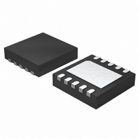
LTC3202EDD Linear Technology, LTC3202EDD Datasheet - Page 2

LTC3202EDD
Manufacturer Part Number
LTC3202EDD
Description
IC LED DRIVR WHITE BCKLGT 10-DFN
Manufacturer
Linear Technology
Type
Backlight, White LEDr
Datasheet
1.LTC3202EDDPBF.pdf
(12 pages)
Specifications of LTC3202EDD
Topology
PWM, Switched Capacitor (Charge Pump)
Number Of Outputs
1
Internal Driver
Yes
Type - Primary
Backlight
Type - Secondary
White LED
Frequency
1.5MHz
Voltage - Supply
2.7 V ~ 4.5 V
Mounting Type
Surface Mount
Package / Case
10-DFN
Operating Temperature
-40°C ~ 85°C
Current - Output / Channel
125mA
Internal Switch(s)
Yes
Lead Free Status / RoHS Status
Contains lead / RoHS non-compliant
Voltage - Output
-
Efficiency
-
Available stocks
Company
Part Number
Manufacturer
Quantity
Price
Company:
Part Number:
LTC3202EDD
Manufacturer:
LT
Quantity:
10 000
Part Number:
LTC3202EDD#PBF
Manufacturer:
LINEAR/凌特
Quantity:
20 000
Company:
Part Number:
LTC3202EDD#TR
Manufacturer:
LT
Quantity:
1 200
Company:
Part Number:
LTC3202EDD#TRPBF
Manufacturer:
LT
Quantity:
5 123
ABSOLUTE AXI U RATI GS
LTC3202
V
D0, D1 ............................................. –0.3V to V
V
I
temperature range, otherwise specifications are at T
PARAMETER
Input Power Supply
V
I
I
Feedback Pin Set Points
0.2V Setting Feedback Voltage
0.4V Setting Feedback Voltage
0.6V Setting Feedback Voltage
I
Charge Pump
R
V
CLK Frequency
D0, D1
High Level Input Voltage (V
Low Level Input Voltage (V
Input Current (I
Input Current (I
Note 1: Absolute Maximum Ratings are those values beyond which the life
of a device may be impaired.
Note 2: Based on long-term current density limitations.
2
PACKAGE/ORDER I FOR ATIO
Consult LTC Marketing for parts specified with wider operating temperature ranges.
ELECTRICAL CHARACTERISTICS
CC
SHDN
FB
OUT
IN
OUT
OL
IN
OUT
Operating Current
Operating Voltage
, V
Open Loop Output Impedance (1.5V
Load Regulation ( V
V
GND
Shutdown Current
(Note 2)....................................................... 150mA
OUT
V
Short-Circuit Duration ............................. Indefinite
D1
OUT
FB
IN
T
JMAX
10-LEAD PLASTIC MSOP
1
2
3
4
5
to GND ......................................... –0.3V to 6V
= 150 C,
MS PACKAGE
IH
IL
TOP VIEW
)
)
JA
W
= 120 C/W
OUT
IL
IH
)
)
/ I
10
9
8
7
6
OUT
D0
C2
C1
C1
C2
+
+
–
–
W W
)
IN
U
– V
OUT
MS PART MARKING
)/I
LTC3202EMS
ORDER PART
OUT
NUMBER
W
LTWL
U
A
CONDITIONS
I
V
D0 = 1, D1 = 0, I
D0 = 0, D1 = 1, I
D0 = 1, D1 = 1, I
V
V
I
DO, D1 = V
DO, D1 = 0V
OUT
OUT
OUT
FB
IN
= 25 C. V
IN
= 3.3V, V
= 0.8V
= 0mA, V
= 10mA to 90mA, V
= 0V
+ 0.3V
The
U
(Note 1)
IN
IN
OUT
OUT
denotes the specifications which apply over the full operating
= 3.3V unless otherwise noted.
OUT
OUT
OUT
= 4.4V, V
= 3.6V, V
Note 3: The LTC3202E is guaranteed to meet performance specifications
from 0 C to 70 C. Specifications over the –40 C to 85 C operating
temperature range are assured by design, characterization and correlation
with statistical process controls.
Operating Temperature Range (Note 3) ...–40 C to 85 C
Storage Temperature Range ..................–65 C to 150 C
Lead Temperature (Soldering, 10 sec).................. 300 C
= 0mA, V
= 0mA, V
= 0mA, V
T
EXPOSED PAD IS PGND (PIN 11) MUST BE
SGND
JMAX
V
10-LEAD (3mm 3mm) PLASTIC DFN
OUT
V
D1
FB
CONNECTED TO GROUND PLANE
IN
FB
FB
= 150 C,
IN
/ V
= 0
1
2
3
4
5
= D0 = D1 = 4.5V
IN
IN
IN
OUT
= 3.6V
= 3.6V
= 3.6V
DD PACKAGE
TOP VIEW
JA
= 1
= 44 C/W,
11
JC
10
9
8
7
6
= 3 C/W
D0
C2
C1
C1
C2
+
+
–
–
MIN
–50
188
380
570
2.7
1.3
–1
–1
DD PART MARKING
0.35
TYP
200
400
600
4.5
1.5
ORDER PART
2.5
LTC3202EDD
NUMBER
LABB
MAX
212
420
630
4.5
0.4
50
5
1
6
1
1
mV/mA
UNITS
3202fa
MHz
mA
mV
mV
mV
nA
V
A
V
V
A
A


