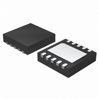
LTC3202EDD Linear Technology, LTC3202EDD Datasheet - Page 6

LTC3202EDD
Manufacturer Part Number
LTC3202EDD
Description
IC LED DRIVR WHITE BCKLGT 10-DFN
Manufacturer
Linear Technology
Type
Backlight, White LEDr
Datasheet
1.LTC3202EDDPBF.pdf
(12 pages)
Specifications of LTC3202EDD
Topology
PWM, Switched Capacitor (Charge Pump)
Number Of Outputs
1
Internal Driver
Yes
Type - Primary
Backlight
Type - Secondary
White LED
Frequency
1.5MHz
Voltage - Supply
2.7 V ~ 4.5 V
Mounting Type
Surface Mount
Package / Case
10-DFN
Operating Temperature
-40°C ~ 85°C
Current - Output / Channel
125mA
Internal Switch(s)
Yes
Lead Free Status / RoHS Status
Contains lead / RoHS non-compliant
Voltage - Output
-
Efficiency
-
Available stocks
Company
Part Number
Manufacturer
Quantity
Price
Company:
Part Number:
LTC3202EDD
Manufacturer:
LT
Quantity:
10 000
Part Number:
LTC3202EDD#PBF
Manufacturer:
LINEAR/凌特
Quantity:
20 000
Company:
Part Number:
LTC3202EDD#TR
Manufacturer:
LT
Quantity:
1 200
Company:
Part Number:
LTC3202EDD#TRPBF
Manufacturer:
LT
Quantity:
5 123
OPERATIO
LTC3202
The LTC3202 uses a fractional conversion switched ca-
pacitor charge pump to boost V
the input voltage. A two-phase nonoverlapping clock acti-
vates the charge pump switches. On the first phase of the
clock the flying capacitors are charged in series from V
On the second phase of the clock they are connected in
parallel and stacked on top of V
charging and discharging the flying capacitors continues
at a free running frequency of 1.5MHz (typ).
Regulation is achieved by sensing the voltage at the FB pin
and modulating the charge pump strength based on the
error signal. The control pins, D0 and D1, program the set
point of the internal digital-to-analog converter. The regu-
lation loop will increase V
the set-point voltage. Table 1 shows the regulation voltage
as a function of D0 and D1.
Table 1. Feedback Control Voltage Settings
In shutdown mode all circuitry is turned off and the
LTC3202 draws only leakage current from the V
Furthermore, V
D1 pins are CMOS inputs with a threshold voltage of
approximately 0.8V. The LTC3202 is in shutdown when a
logic low is applied to both D0 and D1. Since the D0 and D1
pins are high impedance CMOS inputs they should never
be allowed to float. To ensure that their states are defined
they must always be driven with valid logic levels.
Shutdown Current
Output voltage detection circuitry will draw a current of
5 A when the LTC3202 is in shutdown. This current will be
eliminated when the output voltage (V
ensure that V
be used from V
Short-Circuit/Thermal Protection
The LTC3202 has built-in short-circuit current limiting as
well as over temperature protection. During short-circuit
6
D1
0
0
1
1
OUT
OUT
OUT
is at 0V in shutdown a bleed resistor can
U
is disconnected from V
to GND. 10k to 100k is acceptable.
(Refer to Simplified Block Diagram)
D0
0
1
0
1
OUT
until FB comes to balance at
OUT
Feedback Set Point Voltage
to as much as 1.5 times
IN
. This sequence of
OUT
Shutdown
IN
0.2V
0.4V
0.6V
) is at 0V. To
. The D0 and
IN
supply.
IN
.
conditions it will automatically limit its output current to
approximately 250mA. At higher temperatures, or if the
input voltage is high enough to cause excessive self
heating on-chip, thermal shutdown circuitry will
shut down the charge pump when the junction tempera-
ture exceeds approximately 160 C. It will reenable the
charge pump once the junction temperature drops back to
approximately 155 C. The LTC3202 will cycle in and out of
thermal shutdown indefinitely without latchup or damage
until the short-circuit on V
Soft-Start
To prevent excessive current flow at V
the LTC3202 has built-in soft-start circuitry. Soft-start is
achieved by increasing the amount of current available to
the output charge storage capacitor linearly over a period
of approximately 500 s.
The soft-start feature activates any time an input, D0 or D1,
changes state. This will prevent large inrush current
during initial start-up as well as when the feedback setting
is changed from one value to the next. Note that the set
point voltage will drop to zero during the soft-start period.
Under heavy load conditions there may be observable
droop at V
Programming the LTC3202 for Voltage or Current
The LTC3202 can be configured to control either a voltage
or a current. In white LED applications the LED current is
programmed by the ratio of the feedback set point voltage
and a sense resistor as shown in Figure 1. The current of
the remaining LEDs is controlled by virtue of their similar-
ity to the reference LED and the ballast voltage across the
sense resistor.
OUT
LTC3202
GND
until the soft-start circuit catches up.
Figure 1. Current Control Mode
V
5, 11
OUT
FB
3
2
1 F
OUT
I
LED
=
is removed.
V
R
R
FB
X
X
• • •
IN
during start-up,
3202 F01
R
X
3202fa


