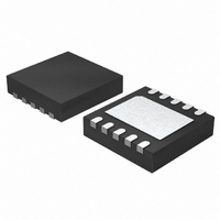
LTC3202EDD Linear Technology, LTC3202EDD Datasheet - Page 7

LTC3202EDD
Manufacturer Part Number
LTC3202EDD
Description
IC LED DRIVR WHITE BCKLGT 10-DFN
Manufacturer
Linear Technology
Type
Backlight, White LEDr
Datasheet
1.LTC3202EDDPBF.pdf
(12 pages)
Specifications of LTC3202EDD
Topology
PWM, Switched Capacitor (Charge Pump)
Number Of Outputs
1
Internal Driver
Yes
Type - Primary
Backlight
Type - Secondary
White LED
Frequency
1.5MHz
Voltage - Supply
2.7 V ~ 4.5 V
Mounting Type
Surface Mount
Package / Case
10-DFN
Operating Temperature
-40°C ~ 85°C
Current - Output / Channel
125mA
Internal Switch(s)
Yes
Lead Free Status / RoHS Status
Contains lead / RoHS non-compliant
Voltage - Output
-
Efficiency
-
Available stocks
Company
Part Number
Manufacturer
Quantity
Price
Company:
Part Number:
LTC3202EDD
Manufacturer:
LT
Quantity:
10 000
Part Number:
LTC3202EDD#PBF
Manufacturer:
LINEAR/凌特
Quantity:
20 000
Company:
Part Number:
LTC3202EDD#TR
Manufacturer:
LT
Quantity:
1 200
Company:
Part Number:
LTC3202EDD#TRPBF
Manufacturer:
LT
Quantity:
5 123
OPERATIO
In this configuration the feedback factor ( V
be very near unity since the small signal LED impedance
will be considerably less than the current setting resistor
R
giving it the lowest closed-loop output resistance. Like-
wise it will also require the largest amount of output
capacitance to preserve stability.
For fixed voltage applications, the output voltage can be
set by the ratio of two resistors and the feedback control
voltage as shown in Figure 2. The output voltage is given
by the set point voltage times the gain factor 1 + R
Note that the closed-loop output resistance will increase in
proportion to the loop gain consumed by the resistive
divider ratio. For example, if the resistor ratio is 2:1 giving
a gain of 3, the closed-loop output resistance will be about
3 times higher than its nominal gain of 1 value. Given that
the closed-loop output resistance is about 0.35 with a
gain of 1, the closed-loop output resistance will be about
1 when using a gain of 3.
When using the LTC3202 in voltage control mode, any of
the three voltage settings (0.2V, 0.4V or 0.6V) can be used
as the set point voltage. For optimum noise performance
and lowest closed-loop output resistance the highest
voltage setting will likely be the most desirable.
Typical values for total voltage divider resistance can
range from several k s up to 1M .
X
. Thus, this configuration will have the highest loop gain
LTC3202
Figure 2. Voltage Control Mode
GND
V
5, 11
OUT
U
FB
3
2
(Refer to Simplified Block Diagram)
1 F
V
OUT
3202 F02
= V
R1
R2
FB
(1 +
R1
R2
FB
)
/ V
OUT
1
) will
/R
2
.
Charge Pump Strength
Figure 3 shows how the LTC3202 can be modeled as a
Thevenin equivalent circuit to determine the amount of
current available from the effective input voltage, 1.5V
and the effective open-loop output resistance, R
From Figure 3 the available current is given by:
Typical values of R
shown in Figure 4.
I
OUT
1 5 .
Figure 3. Equivalent Open-Loop Circuit
4.8
4.6
4.4
4.2
4.0
3.8
Figure 4. Typical R
–40
V
IN
R
V
I
C1 = C2 = 1 F
R
L
FB
OL
OL
= 100mA
V
–
= 0
= (1.5V
IN
–15
V
OL
= 2.7V
OUT
+
–
IN
as a function of temperature are
TEMPERATURE ( C)
1.5V
R
– V
OL
10
IN
OUT
OL
)/I
V
IN
L
vs Temperature
= 3.6V
35
3202 F03
V
OUT
+
–
60
LTC3202
3202 F04
85
OL
.
3202fa
7
IN


