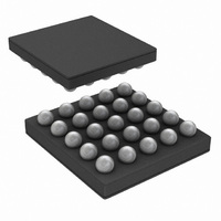
LP5520TL/NOPB National Semiconductor, LP5520TL/NOPB Datasheet - Page 13

LP5520TL/NOPB
Manufacturer Part Number
LP5520TL/NOPB
Description
IC LED DRIVER RGB 25-USMD
Manufacturer
National Semiconductor
Series
PowerWise®r
Type
RGB LED Driverr
Datasheet
1.LP5520TLNOPB.pdf
(34 pages)
Specifications of LP5520TL/NOPB
Constant Current
Yes
Topology
PWM, Step-Up (Boost)
Number Of Outputs
3
Internal Driver
Yes
Type - Primary
Backlight, Light Management Unit (LMU)
Type - Secondary
RGB, White LED
Frequency
1.22kHz, 19.52kHz
Voltage - Supply
2.9 V ~ 5.5 V
Voltage - Output
5 V ~ 20 V
Mounting Type
Surface Mount
Package / Case
25-MicroSMD
Operating Temperature
-30°C ~ 85°C
Current - Output / Channel
60mA
Internal Switch(s)
Yes
Efficiency
87%
Lead Free Status / RoHS Status
Lead free / RoHS Compliant
Other names
LP5520TLTR
The EEPROM data can be read, written and erased through
the serial interface. The boost converter is used to generate
the write and erase voltage for the memory. All operations are
done in page mode. The page address has to be written in
the EEPROM_control register before access to the EEP-
ROM. Incremental access can be used both in I2C and SPI
modes to speed up access. During EEPROM access the
<rgb_auto> control bit in rgb control register must be low.
The EEPROM has 4 pages; only one page at time can be
mirrored at the register map. For getting access to page, the
number of page must be set by <ee_page[1:0]> bits in the
EEPROM_control register(0DH). The page register address
range is from 40H to 5FH.
EEPROM content is copied into SRAM always when the chip
is taken from stand-by mode to active mode. Copying to
SRAM can also be made during operation by writing the
<ee_read> bit high and low in the EEPROM control (0DH)
register. For reading the data from the SRAM, the page num-
ber must be set with <ee_page[1:0]> bits and the page read
from addresses 40H – 5FH.
The EEPROM must be erased before programming. The
erase command will erase one page at time, which must be
selected with <ee_page[1:0]> bits. This operation starts after
setting and resetting <ee_erase> and takes about 100 ms
after rising <ee_erase> bit. During erasing <ee_prog> bit of
the EEPROM_CONTROL register is low. Corresponding
SRAM area will be erased with this operation also.
13
Actually the EEPROM consist of two type of memory, 128 x
8 EEPROM (Non Volatile Memory) and 128 x 8 SRAM (Syn-
chronous Random Access Memory). The EEPROM is used
to store calibrated RGB control values when the system is
powered off. SRAM is used as working memory during oper-
ation.
<ee_erase> and <ee_prog> can be set only one command
at a time (erase or program).
During programming the content of SRAM is copied to EEP-
ROM. EEPROM programming cycle has two steps. At first,
write the whole content of the SRAM, all 4 pages. The whole
page can be written during one SPI/I
crement mode. Second step is programming the EEPROM.
This operation starts after writing <ee_prog> high and back
low and takes about 100 ms after rising <ee_prog> bit. During
programming <ee_prog> bit of the EEPROM_CONTROL
register is low. For EEPROM erasing and programming the
chip has to be in active mode (<NSTBY> high), the boost must
be off (<in_boost> low) and the boost voltage set to 18V
(boost output register value 12H).
<ee_page[1:0]>
(bits1-0)
00
01
10
11
page0 (00H-1FH)
page1 (20H-3FH)
page2 (40H-5FH)
page3 (60H-7FH)
2
C cycle in the auto-in-
20186116
www.national.com


