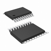
LM3424MH/NOPB National Semiconductor, LM3424MH/NOPB Datasheet - Page 11

LM3424MH/NOPB
Manufacturer Part Number
LM3424MH/NOPB
Description
IC LED DVR BUCK/BOOST 20-TSSOP
Manufacturer
National Semiconductor
Series
PowerWise®r
Type
High Power, Constant Currentr
Datasheet
1.LM3424MHNOPB.pdf
(50 pages)
Specifications of LM3424MH/NOPB
Constant Current
Yes
Topology
Flyback, PWM, SEPIC, Step-Down (Buck), Step-Up (Boost)
Number Of Outputs
1
Internal Driver
No
Type - Primary
Automotive
Type - Secondary
High Brightness LED (HBLED)
Frequency
2MHz
Voltage - Supply
4.5 V ~ 75 V
Mounting Type
Surface Mount
Package / Case
20-TSSOP Exposed Pad, 20-eTSSOP, 20-HTSSOP
Operating Temperature
-40°C ~ 125°C
Current - Output / Channel
1A
Internal Switch(s)
Yes
Efficiency
96%
Lead Free Status / RoHS Status
Lead free / RoHS Compliant
Voltage - Output
-
Other names
LM3424MH
CURRENT REGULATORS
Current regulators can be designed to accomplish three basic
functions: buck, boost, and buck-boost. All three topologies
in their most basic form contain a main switching MosFET, a
recirculating diode, an inductor and capacitors. The LM3424
is designed to drive a ground referenced NFET which is per-
fect for a standard boost regulator. Buck and buck-boost
regulators, on the other hand, usually have a high-side switch.
When driving an LED load, a ground referenced load is often
not necessary, therefore a ground referenced switch can be
used to drive a floating load instead. The LM3424 can then
be used to drive all three basic topologies as shown in the
Basic Topology Schematics section. Other topologies such
as the SEPIC and flyback converter (both derivatives of the
buck-boost) can be implemented as well.
Looking at the buck-boost design, the basic operation of a
current regulator can be analyzed. During the time that the
NFET (Q1) is turned on (t
energy in the inductor (L1) while the output capacitor (C
provides energy to the LED load. When Q1 is turned off
(t
and L1 provides energy to both C
1
operating in CCM.
The average output LED current (I
average inductor current (I
trolled, I
input voltage or output voltage, the ideal duty cycle (D) is var-
ied to regulate I
D is a function of the conversion ratio:
Buck
Boost
Buck-boost
OFF
shows the inductor current (i
), the re-circulating diode (D1) becomes forward biased
LED
will be well regulated. As the system changes
L
and ultimately I
ON
L
), the input voltage source stores
) , therefore if I
L
LED
(t)) waveform for a regulator
O
. For any current regulator,
LED
and the LED load.
FIGURE 1. Ideal CCM Regulator Inductor Current i
) is proportional to the
L
is tightly con-
Figure
O
)
11
PEAK CURRENT MODE CONTROL
Peak current mode control is used by the LM3424 to regulate
the average LED current through an array of HBLEDs. This
method of control uses a series resistor in the LED path to
sense LED current and can use either a series resistor in the
MosFET path or the MosFET R
current limit and input voltage feed forward. The controller has
a fixed switching frequency set by an internal programmable
oscillator which means current mode instability can occur at
duty cycles higher than 50%. To mitigate this standard prob-
lem, an aritifical ramp is added to the control signal internally.
The slope of this ramp is programmable to allow for a wider
range of component choices for a given design. A detailed
explanation of this control method is presented in the follow-
ing sections.
SWITCHING FREQUENCY
The switching frequency of the LM3424 is programmed using
an external resistor (R
as shown in
Alternatively, an external PWM signal can be applied to the
RT pin through a filter (R
capacitor (C
as shown in
a frequency higher than the base frequency set by the R
sistor, the internal oscillator is bypassed and the switching
frequency becomes the synchronized frequency. The exter-
nal synchronization signal should have a pulse width of
100ns, an amplitude between 3V and 6V, and be AC coupled
to the RT pin with a ceramic capacitor (C
10MHz RC filter (R
placed between the PWM signal and C
wanted high frequency noise from coupling into the RT pin.
The switching frequency is defined:
See the Typical Performance Characteristics section for a plot
of R
T
vs. f
SW
AC
Figure
Figure
.
) to synchronize the part to an external clock
FLT
2. If the external PWM signal is applied at
2.
L
(t)
T
= 150Ω and C
) connected from the RT pin to GND
FLT
and C
DS-ON
FLT
30085798
FLT
for both cycle-by-cycle
) and an AC coupling
= 100 pF) should be
AC
to eliminate un-
AC
= 100pF). A
www.national.com
T
re-


