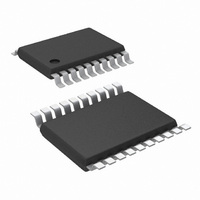
LM3424MH/NOPB National Semiconductor, LM3424MH/NOPB Datasheet - Page 15

LM3424MH/NOPB
Manufacturer Part Number
LM3424MH/NOPB
Description
IC LED DVR BUCK/BOOST 20-TSSOP
Manufacturer
National Semiconductor
Series
PowerWise®r
Type
High Power, Constant Currentr
Datasheet
1.LM3424MHNOPB.pdf
(50 pages)
Specifications of LM3424MH/NOPB
Constant Current
Yes
Topology
Flyback, PWM, SEPIC, Step-Down (Buck), Step-Up (Boost)
Number Of Outputs
1
Internal Driver
No
Type - Primary
Automotive
Type - Secondary
High Brightness LED (HBLED)
Frequency
2MHz
Voltage - Supply
4.5 V ~ 75 V
Mounting Type
Surface Mount
Package / Case
20-TSSOP Exposed Pad, 20-eTSSOP, 20-HTSSOP
Operating Temperature
-40°C ~ 125°C
Current - Output / Channel
1A
Internal Switch(s)
Yes
Efficiency
96%
Lead Free Status / RoHS Status
Lead free / RoHS Compliant
Voltage - Output
-
Other names
LM3424MH
CURRENT SENSE/CURRENT LIMIT
The LM3424 achieves peak current mode control using a
comparator that monitors the main MosFET (Q1) transistor
current, comparing it with the COMP pin voltage as shown in
Figure
protection function. Current limit is accomplished by a redun-
dant internal current sense comparator. If the voltage at the
current sense comparator input (IS) exceeds 245 mV (typi-
cal), the on cycle is immediately terminated. The IS input pin
has an internal N-channel MosFET which pulls it down at the
conclusion of every cycle. The discharge device remains on
an additional 240 ns (typical) after the beginning of a new cy-
cle to blank the leading edge spike on the current sense
signal. The leading edge blanking (LEB) determines the min-
imum achievable on-time (t
There are two possible methods to sense the transistor cur-
rent. The R
the current sense resistance because the IS pin was designed
to withstand the high voltages present on the drain when the
MosFET is in the off state. Alternatively, a sense resistor lo-
cated in the source of the MosFET may be used for current
sensing, however a low inductance (ESL) type is suggested.
The cycle-by-cycle current limit (I
either method as the limiting resistance (R
In general, the external series resistor allows for more design
flexibility, however it is important to ensure all of the noise
sensitive low power ground connections are connected to-
gether local to the controller and a single connection is made
to GND.
FIGURE 7. Current Sense / Current Limit Circuitry
7. Further, it incorporates a cycle-by-cycle over-current
DS-ON
of the main power MosFET can be used as
ON-MIN
LIM
).
) can be calculated using
LIM
):
300857a2
15
SLOPE COMPENSATION
The LM3424 has programmable slope compensation in order
to provide stability over a wide range of operating conditions.
Without slope compensation, a well-known condition called
current mode instability (or sub-harmonic oscillation) can re-
sult if there is a perturbation of the MosFET current sense
voltage at the IS pin, due to noise or a some type of transient.
Through a mathematical / geometrical analysis of the inductor
current (I
be shown that if D < 0.5, the effect of the perturbation will
decrease each switching cycle and the system will remain
stable. However, if D > 0.5 then the perturbation will grow as
shown in
fect where the effect of the perturbation remains, yielding
current mode instability.
Looking at
IS voltage, a mirror of I
offset. The negative input of the PWM comparator is the
COMP pin which is proportional to I
the main MosFET (Q1) is turned off.
The LM3424 mitigates current mode instability by implement-
ing an aritifical ramp (commonly called slope compensation)
which is summed with the sensed MosFET current at the IS
pin as shown in
to the COMP pin to generate the PWM signal. An increase in
the ramp that is added to the sense voltage will increase the
maximum achievable duty cycle. It should be noted that as
the artificial ramp is increased more and more, the control
method approaches standard voltage mode control and the
benefits of current mode control are reduced.
To program the slope compensation, an external resistor,
R
of the artificial ramp that is added to the MosFET current
sense voltage. A smaller R
the added ramp. A simple calculation is suggested to ensure
any duty cycle is attainable while preventing the addition of
excessive ramp. This method requires the artifical ramp slope
(M
SLP
A
FIGURE 8. "Period Doubling" due to Current Mode
) to be equal to half the inductor slope during t
, is connected from SLOPE to GND. This sets the slope
L
Figure
) and the corresponding control current (I
Figure
Figure
8, eventually causing a "period doubling" ef-
7, the positive PWM comparator input is the
7. This combined signal is compared
L
Instability
during t
SLP
value will increase the slope of
ON
C
, plus a typical 900 mV
, the threshold at which
www.national.com
OFF
C
:
, it can
30085706


