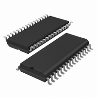
PCA9625D/S911,518 NXP Semiconductors, PCA9625D/S911,518 Datasheet - Page 13

PCA9625D/S911,518
Manufacturer Part Number
PCA9625D/S911,518
Description
IC LED DRIVER RGBA 32-SOIC
Manufacturer
NXP Semiconductors
Type
RGBA LED Driverr
Datasheet
1.PCA9625D512.pdf
(33 pages)
Specifications of PCA9625D/S911,518
Topology
Open Drain, PWM
Number Of Outputs
16
Internal Driver
Yes
Type - Primary
Backlight, LED Blinker
Type - Secondary
RGBA
Frequency
1MHz
Voltage - Supply
2.3 V ~ 5.5 V
Voltage - Output
24V
Mounting Type
Surface Mount
Package / Case
32-SOIC (7.5mm Width)
Operating Temperature
-40°C ~ 85°C
Current - Output / Channel
100mA
Internal Switch(s)
Yes
Lead Free Status / RoHS Status
Lead free / RoHS Compliant
Efficiency
-
Other names
935285147518
PCA9625D/S911-T
PCA9625D/S911-T
PCA9625D/S911-T
PCA9625D/S911-T
NXP Semiconductors
PCA9625_2
Product data sheet
7.3.6 LEDOUT0 to LEDOUT3, LED driver output state
7.3.7 SUBADR1 to SUBADR3, I
Table 10.
Legend: * default value.
LDRx = 00 — LED driver x is off (default power-up state).
LDRx = 01 — LED driver x is fully on (individual brightness and group dimming/blinking
not controlled).
LDRx = 10 — LED driver x individual brightness can be controlled through its PWMx
register.
LDRx = 11 — LED driver x individual brightness and group dimming/blinking can be
controlled through its PWMx register and the GRPPWM registers.
Table 11.
Legend: * default value.
Subaddresses are programmable through the I
E4h, E8h, and the device(s) will not acknowledge these addresses right after power-up
(the corresponding SUBx bit in MODE1 register is equal to 0).
Address
14h
15h
16h
17h
Address
18h
19h
1Ah
Register
SUBADR1
SUBADR2
SUBADR3
LEDOUT0 to LEDOUT3 - LED driver output state register (address 14h to 17h) bit
description
Register
LEDOUT0
LEDOUT1
LEDOUT2
LEDOUT3
SUBADR1 to SUBADR3 - I
1Ah) bit description
Rev. 02 — 15 January 2008
Bit
7:6
5:4
3:2
1:0
7:6
5:4
3:2
1:0
7:6
5:4
3:2
1:0
7:6
5:4
3:2
1:0
Bit
7:1
0
7:1
0
7:1
0
Symbol
LDR3
LDR2
LDR1
LDR0
LDR7
LDR6
LDR5
LDR4
LDR11
LDR10
LDR9
LDR8
LDR15
LDR14
LDR13
LDR12
2
C-bus subaddress 1 to 3
Symbol
A1[7:1]
A1[0]
A2[7:1]
A2[0]
A3[7:1]
A3[0]
2
C-bus subaddress registers 0 to 3 (address 18h to
Access Value
R/W
R/W
R/W
R/W
R/W
R/W
R/W
R/W
R/W
R/W
R/W
R/W
R/W
R/W
R/W
R/W
Access Value
R/W
R only
R/W
R only
R/W
R only
16-bit Fm+ I
2
C-bus. Default power-up values are E2h,
00*
00*
00*
00*
00*
00*
00*
00*
00*
00*
00*
00*
00*
00*
00*
00*
1110 001*
0*
1110 010*
0*
1110 100*
0*
2
C-bus 100 mA 24 V LED driver
Description
LED3 output state control
LED2 output state control
LED1 output state control
LED0 output state control
LED7 output state control
LED6 output state control
LED5 output state control
LED4 output state control
LED11 output state control
LED10 output state control
LED9 output state control
LED8 output state control
LED15 output state control
LED14 output state control
LED13 output state control
LED12 output state control
Description
I
reserved
I
reserved
I
reserved
2
2
2
C-bus subaddress 1
C-bus subaddress 2
C-bus subaddress 3
PCA9625
© NXP B.V. 2008. All rights reserved.
13 of 33


