ISL6612BCBZ Intersil, ISL6612BCBZ Datasheet
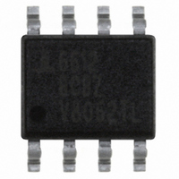
IC DRIVER MOSFET SYNC BUCK 8SOIC

ISL6612BCBZ

Manufacturer Part Number
ISL6612BCBZ
Description
IC DRIVER MOSFET SYNC BUCK 8SOIC
Manufacturer
Intersil
Datasheet

Specifications of ISL6612BCBZ

Configuration
High and Low Side, Synchronous
Input Type
PWM
Delay Time
10.0ns
Current - Peak
1.25A
Number Of Configurations
1
Number Of Outputs
2
High Side Voltage - Max (bootstrap)
36V
Voltage - Supply
7 V ~ 13.2 V
Operating Temperature
0°C ~ 85°C
Mounting Type
Surface Mount
Package / Case
8-SOIC (3.9mm Width)
Lead Free Status / RoHS Status
Lead free / RoHS Compliant

Available stocks

Company
Part Number
Manufacturer
Quantity
Price
Part Number:
ISL6612BCBZ
Quantity:
5 510
Advanced Synchronous Rectified Buck
MOSFET Drivers with Pre-POR OVP
The ISL6612B and ISL6613B are high frequency MOSFET
drivers specifically designed to drive upper and lower power
N-Channel MOSFETs in a synchronous rectified buck
converter topology. These drivers combined with HIP63xx or
ISL65xx Multi-Phase Buck PWM controllers and N-Channel
MOSFETs form complete core-voltage regulator solutions for
advanced microprocessors.
The ISL6612B drives the upper gate to above rising VCC
POR (7V), while the lower gate can be independently driven
over a range from 5V to 12V. The ISL6613B drives both
upper and lower gates over a range of 5V to 12V. This drive-
voltage provides the flexibility necessary to optimize
applications involving trade-offs between gate charge and
conduction losses. These drivers are optimized for POL
DC/DC Converters for IBA Systems.
An advanced adaptive zero shoot-through protection is
integrated to prevent both the upper and lower MOSFETs
from conducting simultaneously and to minimize the dead
time. These products add an overvoltage protection feature
operational before VCC exceeds its turn-on threshold, at
which the PHASE node is connected to the gate of the low
side MOSFET (LGATE). The output voltage of the converter
is then limited by the threshold of the low side MOSFET,
which provides some protection to the microprocessor if the
upper MOSFET(s) is shorted during initial start-up.
These drivers also feature a three-state PWM input which,
working together with Intersil’s multi-phase PWM controllers,
prevents a negative transient on the output voltage when the
output is shut down. This feature eliminates the Schottky
diode that is used in some systems for protecting the load
from reversed output voltage events.
®
1
Data Sheet
1-888-INTERSIL or 1-888-468-3774
CAUTION: These devices are sensitive to electrostatic discharge; follow proper IC Handling Procedures.
Features
• Pin-to-pin Compatible with HIP6601 SOIC family
• Dual MOSFET Drives for Synchronous Rectified Bridge
• Low VCC Rising Threshold (7V) for IBA Applications.
• Advanced Adaptive Zero Shoot-Through Protection
• Adjustable Gate Voltage (5V to 12V) for Optimal Efficiency
• 36V Internal Bootstrap Schottky Diode
• Bootstrap Capacitor Overcharging Prevention
• Supports High Switching Frequency (up to 2MHz)
• Three-State PWM Input for Output Stage Shutdown
• Three-State PWM Input Hysteresis for Applications With
• Pre-POR Overvoltage Protection
• VCC Undervoltage Protection
• Expandable Bottom Copper Pad for Enhanced Heat
• Dual Flat No-Lead (DFN) Package
• Pb-Free Plus Anneal Available (RoHS Compliant)
Applications
• Optimized for POL DC/DC Converters for IBA Systems
• Core Regulators for Intel
• High Current DC/DC Converters
• High Frequency and High Efficiency VRM and VRD
Related Literature
• Technical Brief TB363 “Guidelines for Handling and
• Technical Brief TB417 for Power Train Design, Layout
- Body Diode Detection
- Auto-zero of r
- 3A Sinking Current Capability
- Fast Rise/Fall Times and Low Propagation Delays
Power Sequencing Requirement
Sinking
- Near Chip-Scale Package Footprint; Improves PCB
Processing Moisture Sensitive Surface Mount Devices
(SMDs)”
Guidelines, and Feedback Compensation Design
Efficiency and Thinner in Profile
All other trademarks mentioned are the property of their respective owners.
July 27, 2006
|
Intersil (and design) is a registered trademark of Intersil Americas Inc.
Copyright Intersil Americas Inc. 2005-2006. All Rights Reserved
DS(ON)
ISL6612B, ISL6613B
Conduction Offset Effect
®
and AMD
®
Microprocessors
FN9205.3

Related parts for ISL6612BCBZ

ISL6612BCBZ Summary of contents

Page 1

... Guidelines, and Feedback Compensation Design CAUTION: These devices are sensitive to electrostatic discharge; follow proper IC Handling Procedures. | 1-888-INTERSIL or 1-888-468-3774 Intersil (and design registered trademark of Intersil Americas Inc. Copyright Intersil Americas Inc. 2005-2006. All Rights Reserved All other trademarks mentioned are the property of their respective owners. FN9205.3 Conduction Offset Effect ® ...

Page 2

... Ordering Information PART NUMBER PART MARKING ISL6612BCB 6612BCB ISL6612BCB-T 6612BCB ISL6612BCBZ (Note) 6612BCBZ ISL6612BCBZ-T (Note) 6612BCBZ ISL6612BCR 12BC ISL6612BCR-T 12BC ISL6612BCRZ (Note) 12BZ ISL6612BCRZ-T (Note) 12BZ ISL6612BECB 6612BECB ISL6612BECB-T 6612BECB ISL6612BECBZ (Note) 6612BECBZ ISL6612BECBZ-T (Note) 6612BECBZ ISL6612BEIB 6612BEIB ISL6612BEIB-T 6612BEIB ISL6612BEIBZ (Note) ...

Page 3

... NOTE: Intersil Pb-free plus anneal products employ special Pb-free material sets; molding compounds/die attach materials and 100% matte tin plate termination finish, which are RoHS compliant and compatible with both SnPb and Pb-free soldering operations. Intersil Pb-free products are MSL classified at Pb-free peak reflow temperatures that meet or exceed the Pb-free requirements of IPC/JEDEC J STD-020. ...

Page 4

Typical Application - 3 Channel Converter Using ISL65xx and ISL6612B Gate Drivers +5V +5V VFB VFB VCC VCC COMP COMP PWM1 PWM1 VSEN VSEN PWM2 PWM2 PGOOD PGOOD PWM3 PWM3 MAIN MAIN CONTROL CONTROL ISL65xx ISL65xx VID VID ISEN1 ISEN1 ...

Page 5

Absolute Maximum Ratings Supply Voltage (VCC .15V Supply ...

Page 6

Electrical Specifications Recommended Operating Conditions, Unless Otherwise Noted. (Continued) PARAMETER Three-State Upper Gate Rising Threshold Three-State Upper Gate Falling Threshold Shutdown Holdoff Time UGATE Rise Time LGATE Rise Time UGATE Fall Time LGATE Fall Time UGATE Turn-On Propagation Delay (Note ...

Page 7

... The Three-State PWM Input PDHL A unique feature of these drivers and other Intersil drivers is the addition of a shutdown window to the PWM input. If the PWM signal enters and remains within the shutdown window for a set holdoff time, the driver outputs are disabled and ], turning on the lower both MOSFET gates are pulled and held low ...

Page 8

This feature helps prevent a negative transient on the output voltage when the output is shut down, eliminating the Schottky diode that is used in some systems for protecting the load from reversed output voltage events. In addition, more than ...

Page 9

MOSFETs. The total gate drive power losses due to the gate charge of MOSFETs and the driver’s internal circuitry and their corresponding average driver current can be estimated with EQs. 2 and 3, respectively, • ...

Page 10

... The pin #1 identifier may be either a mold or mark feature. 7. Dimensions D2 and E2 are for the exposed pads which provide NX b improved electrical and thermal performance Nominal dimensions are provided to assist with PCB Land Pattern Design efforts, see Intersil Technical Brief TB389. 0. 0.200 ...

Page 11

Small Outline Exposed Pad Plastic Packages (EPSOIC) N INDEX 0.25(0.010) H AREA E - TOP VIEW SEATING PLANE - -C- α 0.10(0.004) 0.25(0.010 SIDE VIEW 1 ...

Page 12

... Accordingly, the reader is cautioned to verify that data sheets are current before placing orders. Information furnished by Intersil is believed to be accurate and reliable. However, no responsibility is assumed by Intersil or its subsidiaries for its use; nor for any infringements of patents or other rights of third parties which may result from its use ...

Related keywords