IRS26310DJPBF International Rectifier, IRS26310DJPBF Datasheet
IRS26310DJPBF
Specifications of IRS26310DJPBF
Available stocks


Related parts for IRS26310DJPBF

IRS26310DJPBF Summary of contents
Page 1
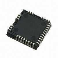
... HIGH VOLTAGE 3 PHASE GATE DRIVER IC WITH DC BUS Product Summary Topology V OFFSET V OUT I & & OFF Deadtime (typical) & Package Options Data Sheet No. PD60347 IRS26310DJPbF OVER –VOLTAGE PROTECTION 3 Phase ≤ 600 – (typical) 200 mA & 350 mA (typical) 530 ns & 530 ns 290 ns 44-Lead PLCC (without 12 leads) ...
Page 2
... Recommended Operating Conditions Static Electrical Characteristics Dynamic Electrical Characteristics Functional Block Diagram Input/Output Pin Equivalent Circuit Diagram Lead Definitions Lead Assignments Application Information and Additional Details Parameter Temperature Trends Package Details Tape and Reel Details Part Marking Information Ordering Information www.irf.com IRS26310DJPbF 2 Page ...
Page 3
... Description The IRS26310DJPBF is a high voltage, high speed power MOSFET and IGBT driver with three independent high and low side referenced output channels for 3-phase applications. This IC is designed to be used with low-cost bootstrap power supplies; the bootstrap diode functionality has been integrated into this device to reduce the component count and the PCB size ...
Page 4
... Typical Application Diagram www.irf.com IRS26310DJPbF 4 © 2007 International Rectifier ...
Page 5
... International Rectifier sales representative for further information. ††† Higher MSL ratings may be available for the specific package types listed here. International Rectifier sales representative for further information. www.irf.com IRS26310DJPbF Industrial Comments: This family of ICs has passed JEDEC’s Industrial qualification. IR’s Consumer qualification level is granted by extension of the higher Industrial level ...
Page 6
... Lead temperature (soldering, 10 seconds) L † All supplies are fully tested internal 20 V clamp exists for each supply. www.irf.com unless otherwise stated in the table. The thermal resistance SS & V (20 V), and V & V (20 V Definition voltage BUS 6 IRS26310DJPbF Min. Max. Units - 20 † 0 -0.3 20 -0.3 620 ...
Page 7
... Application Information section of this datasheet for more details. ††† DCBusSense pin is internally clamped with a 10.4 V zener diode. www.irf.com unless otherwise stated in the table. The offset rating is tested with supplies SS Definition † †† with pulse width. Guaranteed by design. Refer IRS26310DJPbF Min. Max COM-8 600 -50 600 ...
Page 8
... O 10.4 10.2 0.17 10.4 10.2 0.17 3.86 3.70 0.14 — — — — -1 — -1 — -1 — IRS26310DJPbF ,V and I parameters are parameters are referenced to respective O parameters are referenced to CCUV Typ. Max. Units Test Conditions — — — 0.8 1.9 — 1 — — ...
Page 9
... Internal bootstrap diode Ron BS www.irf.com unless otherwise specified. The V and I parameters are referenced to respective Definition Min. — -1 120 250 — — — 9 IRS26310DJPbF ,V and I parameters are referenced parameters are referenced to V CCUV Typ. Max. Units Conditions — 200 — PW ≤ 10 µs ...
Page 10
... OUT 10 IRS26310DJPbF Max. Units Test Conditions 750 750 & 190 75 1200 ITRIP 750 & 950 ITRIP 650 & 5V ...
Page 11
... Functional Block Diagram: IRS26310DJ www.irf.com IRS26310DJPbF © 2008 International Rectifier 11 ...
Page 12
... Input/Output Pin Equivalent Circuit www.irf.com Diagrams: IRS26310D 12 IRS26310DJPbF © 2008 International Rectifier ...
Page 13
... Analog input for DCbus sensing DCbusSense An external RC network input used to define the FAULT CLEAR delay (t equal to R*C. When RCIN > the FAULT pin goes back into an open-drain high-impedance RCIN state. www.irf.com Description , then automatically becomes inactive (open-drain high impedance). 13 IRS26310DJPbF ) approximately FLTCLR © 2008 International Rectifier ...
Page 14
... Lead Assignments www.irf.com IRS26310DJPbF © 2008 International Rectifier 14 ...
Page 15
... OUT ( (or COM) Figure 1: HVIC sourcing current www.irf.com . The voltage that drives the gate of the external power switch is O for the low-side power switch; this parameter is sometimes IRS26310DJPbF (or LO (or COM) Figure 2: HVIC sinking current © 2008 International Rectifier ...
Page 16
... During intervals D and E of Figure 4, we can see that the enable (EN) pin has been pulled low (as is the case when the driver IC has received a command from the control IC to shutdown); this results in the outputs (HOx and LOx) being held in the low state until the enable pin is pulled high. www.irf.com IN Figure 3: Switching time waveforms 16 IRS26310DJPbF , and t ) associated with ...
Page 17
... IRS26310D specifies the maximum difference between DT comparing the DT of one channel of the IRS26310D to that of another. www.irf.com Figure 4: Input/output timing diagram Figure 5: Detailed view of B & C intervals and IRS26310DJPbF . The MDT parameter also applies when 2 © 2008 International Rectifier ...
Page 18
... V and 5 V logic-level signals. Figure 7 illustrates an input signal to the IRS26310D, its input threshold values, and the logic state of the result of the input signal. www.irf.com 50% DT Figure 6: Illustration of deadtime ) of the IRS26310D is matched to the propagation ON Figure 7: HIN & LIN input thresholds 18 IRS26310DJPbF 50 for both ON OFF © 2008 International Rectifier ...
Page 19
... CCUV- voltage fail to reach the V threshold, the IC will not turn-on. Additionally, if the BSUV threshold during operation, the undervoltage lockout circuitry will recognize a BSUV Figure 8: UVLO protection 19 IRS26310DJPbF (logic and low-side circuitry) power the undervoltage protection CCUV+/- BSUV+/- © 2008 International Rectifier ...
Page 20
... Table 2 gives a summary of this pin’s functionality and EN Enable Input Enable input high Outputs enabled Enable input low Outputs disabled Table 2: Enable functionality truth table (*assumes no other fault condition) 20 IRS26310DJPbF Please refer to the EN pin FILTER,EN * © 2008 International Rectifier ...
Page 21
... Figure 10: Output enable/disable timing waveform www.irf.com IRS26310DJPbF © 2008 International Rectifier 21 ...
Page 22
... V RCIN Figure 12: Programming the fault clear timer ≤ RCIN Ceramic 0.5 MΩ MΩ R RCIN >> R ON,RCIN Table 3: Design guidelines -t/ -(R C )ln(1-V FLTCLR RCIN RCIN RCIN,TH 22 IRS26310DJPbF and the RCIN pin, while C CC RCIN / © 2008 International Rectifier is placed ...
Page 23
... IT,TH could be 50 mΩ. The voltage of the ITRIP pin should not be allowed to 0 and the ITRIP functionality by the time that IT,TH+ 23 IRS26310DJPbF . SS ). The circuit designer will need IT,TH and R such that the voltage the temperature changes, the 4 . The resistor values should ...
Page 24
... DC bus voltage and select R voltage at node V reaches the over-voltage threshold (O X www.irf.com Figure 15: Using over-current protection and over- temperature protection VDCBUSVTH- ). VDCBUSVTH /( VDCBUSVTH+ 1 DCBUS IRS26310DJPbF . and 0 ). The circuit VDCBUSVTH+ and R such that the 0 1 © 2008 International Rectifier ...
Page 25
... BSUV VBS ITRIP EN RCIN --- --- --- High --- --- --- High < High BSUV 15 V > Low ITRIP High High 25 IRS26310DJPbF DCbus has been tripped; the CC is not latched in this case and CCUV FAULT returns ITRIP FAULT High High Z LIN High High Z LIN HIN © 2008 International Rectifier ...
Page 26
... FIL,IN ; the resulting output is approximately the difference between the input signal and ; the resulting output is approximately the same duration as the input signal. FIL,IN FIL,IN 26 IRS26310DJPbF ; the resulting output is approximately the FIL,IN ; the resulting output is FIL,IN Figure 18: Advanced input filter ; the output does not change states. Example 2 © ...
Page 27
... ON and narrow OFF cases is shown in OUT IN –PW duration. This data illustrates the performance and near symmetry OUT IN Figure 20: Input filter characteristic 27 IRS26310DJPbF duration. It can be seen that for a PW OUT durations mimic the PW durations very well over IN © 2008 International Rectifier IN , ...
Page 28
... PWM schemes (typically 6-step modulations) and at very www.irf.com , see Figure 22 for an illustration of this internal connection Figure 23: Bootstrap MOSFET state diagram 28 IRS26310DJPbF supply and CC voltage is higher than approximately B returns below that threshold; this B © 2008 International Rectifier ...
Page 29
... LO . G,LO DC+ BUS (x3 (x3) G, (x3 (x3) ITRIP R G, GE1 V - COM DC- BUS Figure 24: Separate V and COM pins SS 29 IRS26310DJPbF and COM respectively) to eliminate some of the in the figure is the voltage between the the low-side switch is the GE2 GE3 - - © 2008 International Rectifier ...
Page 30
... IGBT switches on, the current commutation occurs from D3 to Q4. At the same instance, the voltage node, V swings from the positive DC bus voltage to the negative DC bus voltage. www.irf.com Figure 25: Three phase inverter Figure 27: D2 conducting 30 IRS26310DJPbF , swings from the positive DC bus S1 © 2008 International Rectifier , S2 ...
Page 31
... DC bus, rather it S and L C (the load is not shown in these figures). This current S1 Figure 31: V positive S 31 IRS26310DJPbF Figure 29: Q4 conducting transient”. S for each IGBT. When the high-side switch is on, E pin). S Figure 32: V negative ...
Page 32
... International Rectifier HVIC S ) near the respective high voltage portions of the device. The IRS26310D in the Figure 34: Antenna Loops 32 IRS26310DJPbF transient conditions highly S transients as much as possible by careful PCB S © 2008 International Rectifier ...
Page 33
... V cc HIN (x3) V (x3) B LIN (x3) EN FAULT C IN RCIN LO (x3) ITRIP COM V SS Figure 35: Supply capacitor Figure 37 IRS26310DJPbF ) between the V and V pins. This (x3) V (x3) S spikes remain excessive, further steps S pin and the switch S and V (see Figure 37). See DT04 clamping diode S © ...
Page 34
... Temperature ( Figure 38: t vs. temperature ON 600 450 Exp. 300 150 0 -50 - Temperature ( Figure 40: DT vs. temperature www.irf.com 75 100 125 100 125 IRS26310DJPbF 1000 800 Exp. 600 400 200 0 -50 - Temperature ( C) Figure 39: t vs. temperature OFF 1500 1250 1000 Exp. 750 500 250 0 -50 -25 0 ...
Page 35
... Temperature ( Figure 46: I vs. temperature QCC www.irf.com 500 400 300 200 100 0 75 100 125 o C) 100 100 125 o C) 100 100 125 IRS26310DJPbF Exp. -50 - Temperature ( C) Figure 43: t vs. temperature EN Exp. -50 - Temperature ( C) Figure 45: R vs. temperature ON,FLT Exp. -50 - Temperature ( C) Figure 47: I vs. temperature QBS © 2008 International Rectifier ...
Page 36
... IT,TH+ www.irf.com 20.00 16.00 12.00 8.00 4.00 0. 100 125 25.00 20.00 15.00 10.00 5.00 0. 100 125 1.00 0.80 0.60 0.40 0.20 0.00 75 100 125 36 IRS26310DJPbF Exp. -50 - Temperature (oC) Figure 49: V vs. temperature CCUV- Exp. -50 - Temperature (oC) Figure 51: V vs. temperature BSUV- Exp. -50 - Temperature (oC) Figure 53: V vs. temperature IT,TH- © ...
Page 37
... C) 10.00 8.00 6.00 Exp. 4.00 2.00 0.00 -50 - Temperature ( C) Figure 58: I vs. temperature ITRIP+ 37 IRS26310DJPbF Exp. 0 -50 - Temperature ( C) Figure 55: I vs. temperature O- Figure 57: V vs. temperature DCBUSSTH- 75 100 125 © 2008 International Rectifier 100 125 ...
Page 38
... Package Details: PLCC44 www.irf.com IRS26310DJPbF © 2008 International Rectifier 38 ...
Page 39
... C 12.80 13.20 0.503 D 1.95 2.45 0.767 E 98.00 102.00 3.858 F n/a 38.4 n/a G 34.7 35.8 1.366 H 32.6 33.1 1.283 39 IRS26310DJPbF Imperial Max 0.948 0.161 1.271 0.562 0.712 0.712 n/a 0.062 D A Imperial Max 13.001 0.844 0.519 0.096 4.015 1.511 1.409 1.303 © ...
Page 40
... Part Marking Information www.irf.com IRS26310DJPbF © 2008 International Rectifier 40 ...
Page 41
... For technical support, please contact IR’s Technical Assistance Center www.irf.com Standard Pack Form Tube/Bulk Tape and Reel supersedes and replaces all information previously supplied. http://www.irf.com/technical-info/ WORLD HEADQUARTERS: 233 Kansas St., El Segundo, California 90245 Tel: (310) 252-7105 41 IRS26310DJPbF Complete Part Number Quantity 27 IRS26310DJPBF 500 IRS26310DJTRPBF © 2008 International Rectifier ...