IRS26310DJPBF International Rectifier, IRS26310DJPBF Datasheet - Page 15
IRS26310DJPBF
Manufacturer Part Number
IRS26310DJPBF
Description
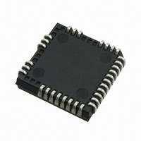
IC DRIVER BRIDGE 3-PHASE 44-PLCC
Manufacturer
International Rectifier
Datasheet
1.IRS26310DJTRPBF.pdf
(41 pages)
Specifications of IRS26310DJPBF
Configuration
3 Phase Bridge
Input Type
Non-Inverting
Delay Time
530ns
Current - Peak
200mA
Number Of Configurations
1
Number Of Outputs
3
High Side Voltage - Max (bootstrap)
600V
Voltage - Supply
12 V ~ 20 V
Operating Temperature
-40°C ~ 125°C
Mounting Type
Surface Mount
Package / Case
44-PLCC (32 Leads)
Peak Output Current
200mA
Input Delay
530ns
Output Delay
530ns
Supply Voltage Range
12V To 20V
Driver Case Style
LCC
No. Of Pins
44
Operating Temperature Range
-40°C To +125°C
Rohs Compliant
Yes
Device Type
High Side / Low Side
Family Hvic
General Purpose HVICs
Channels
6
Topology
Three Phase
Application
General Purpose / Motor Control / PDP
Voffset
600
Io+ (ma)
200
Io- (ma)
350
Shutdown / Reset
Yes
Separate Power And Logic Ground
Yes
Integrated Bootstrap Diode
Yes
Over Current Protection
Yes
Uvlo
Vcc / Vbs
Vbsuv+ / Vccuv+ Min (v)
10.4
Vbsuv+ / Vccuv+ Typ (v)
11.1
Vbsuv+ / Vccuv+ Max (v)
11.6
Vbsuv- / Vccuv- Min (v)
10.2
Vbsuv- / Vccuv- Typ (v)
10.9
Dt / Sdt Min (ns)
190
Dt / Sdt Typ (ns)
290
Dt / Sdt Max (ns)
420
T On Min (ns)
400
T On Typ (ns)
530
T On Max (ns)
750
T Off Min (ns)
400
T Off Typ (ns)
530
T Off Max (ns)
750
Fault Reporting
Yes
Package
44 Lead
Part Status
Active & Preferred
Special Features
DC Bus Sensing with Over Voltage Protection
Lead Free Status / RoHS Status
Lead free / RoHS Compliant
Available stocks
Company
Part Number
Manufacturer
Quantity
Price
Company:

Part Number:
IRS26310DJPBF
Manufacturer:
International Rectifier
Quantity:
10 000


Application Information and Additional Details
Informations regarding the following topics are included as subsections within this section of the datasheet.
IGBT/MOSFET Gate Drive
The IRS26310D HVIC is designed to drive up to six MOSFET or IGBT power devices. Figures 1 and 2 illustrate
several parameters associated with the gate drive functionality of the HVIC. The output current of the HVIC, used to
drive the gate of the power switch, is defined as I
defined as V
generically called V
www.irf.com
•
•
•
•
•
•
•
•
•
•
•
•
•
•
•
•
•
•
•
•
•
IGBT/MOSFET Gate Drive
Switching and Timing Relationships
Deadtime
Matched Propagation Delays
Input Logic Compatibility
Undervoltage Lockout Protection
Shoot-Through Protection
Enable Input
Fault Reporting and Programmable Fault Clear Timer
Over-Current Protection
Over-Temperature Shutdown Protection
DC bus over-voltage Protection
Truth Table: Undervoltage lockout, ITRIP, and ENABLE
Advanced Input Filter
Short-Pulse / Noise Rejection
Integrated Bootstrap Functionality
Bootstrap Power Supply Design
Separate Logic and Power Grounds
Tolerant to Negative V
PCB Layout Tips
Additional Documentation
Figure 1: HVIC sourcing current
(or COM)
HO
(or V
(or LO)
V
for the high-side power switch and V
HO
V
S
B
CC
OUT
)
+
and in this case does not differentiate between the high-side or low-side output voltage.
V
-
HO
(or V
S
Transients
LO
I
O+
)
O
. The voltage that drives the gate of the external power switch is
LO
for the low-side power switch; this parameter is sometimes
15
Figure 2: HVIC sinking current
(or COM)
(or V
(or LO)
V
HO
V
S
B
CC
)
IRS26310DJPbF
© 2008 International Rectifier
I
O-
Related parts for IRS26310DJPBF
Image
Part Number
Description
Manufacturer
Datasheet
Request
R

Part Number:
Description:
SCHOTTKY RECTIFIER
Manufacturer:
International Rectifier Corp.
Datasheet:
Part Number:
Description:
SCHOTTKY RECTIFIER
Manufacturer:
International Rectifier Corp.
Datasheet:
Part Number:
Description:
SCHOTTKY RECTIFIER
Manufacturer:
International Rectifier Corp.
Datasheet:
Part Number:
Description:
SCHOTTKY RECTIFIER
Manufacturer:
International Rectifier Corp.
Datasheet:
Part Number:
Description:
SCHOTTKY RECTIFIER
Manufacturer:
International Rectifier Corp.
Datasheet:
Part Number:
Description:
SCHOTTKY RECTIFIER
Manufacturer:
International Rectifier Corp.
Datasheet:
Part Number:
Description:
SCHOTTKY RECTIFIER
Manufacturer:
International Rectifier Corp.
Datasheet:
Part Number:
Description:
SCHOTTKY RECTIFIER
Manufacturer:
International Rectifier Corp.
Datasheet:
Part Number:
Description:
SCHOTTKY RECTIFIER
Manufacturer:
International Rectifier Corp.
Datasheet:
Part Number:
Description:
SCHOTTKY RECTIFIER
Manufacturer:
International Rectifier Corp.
Datasheet:
Part Number:
Description:
SCHOTTKY RECTIFIER
Manufacturer:
International Rectifier Corp.
Datasheet:
Part Number:
Description:
SCHOTTKY RECTIFIER
Manufacturer:
International Rectifier Corp.
Datasheet:
Part Number:
Description:
SCHOTTKY RECTIFIER
Manufacturer:
International Rectifier Corp.
Datasheet:
Part Number:
Description:
SCHOTTKY RECTIFIER
Manufacturer:
International Rectifier Corp.
Datasheet:
Part Number:
Description:
SCHOTTKY RECTIFIER
Manufacturer:
International Rectifier Corp.
Datasheet: