IRS26310DJPBF International Rectifier, IRS26310DJPBF Datasheet - Page 31
IRS26310DJPBF
Manufacturer Part Number
IRS26310DJPBF
Description
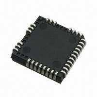
IC DRIVER BRIDGE 3-PHASE 44-PLCC
Manufacturer
International Rectifier
Datasheet
1.IRS26310DJTRPBF.pdf
(41 pages)
Specifications of IRS26310DJPBF
Configuration
3 Phase Bridge
Input Type
Non-Inverting
Delay Time
530ns
Current - Peak
200mA
Number Of Configurations
1
Number Of Outputs
3
High Side Voltage - Max (bootstrap)
600V
Voltage - Supply
12 V ~ 20 V
Operating Temperature
-40°C ~ 125°C
Mounting Type
Surface Mount
Package / Case
44-PLCC (32 Leads)
Peak Output Current
200mA
Input Delay
530ns
Output Delay
530ns
Supply Voltage Range
12V To 20V
Driver Case Style
LCC
No. Of Pins
44
Operating Temperature Range
-40°C To +125°C
Rohs Compliant
Yes
Device Type
High Side / Low Side
Family Hvic
General Purpose HVICs
Channels
6
Topology
Three Phase
Application
General Purpose / Motor Control / PDP
Voffset
600
Io+ (ma)
200
Io- (ma)
350
Shutdown / Reset
Yes
Separate Power And Logic Ground
Yes
Integrated Bootstrap Diode
Yes
Over Current Protection
Yes
Uvlo
Vcc / Vbs
Vbsuv+ / Vccuv+ Min (v)
10.4
Vbsuv+ / Vccuv+ Typ (v)
11.1
Vbsuv+ / Vccuv+ Max (v)
11.6
Vbsuv- / Vccuv- Min (v)
10.2
Vbsuv- / Vccuv- Typ (v)
10.9
Dt / Sdt Min (ns)
190
Dt / Sdt Typ (ns)
290
Dt / Sdt Max (ns)
420
T On Min (ns)
400
T On Typ (ns)
530
T On Max (ns)
750
T Off Min (ns)
400
T Off Typ (ns)
530
T Off Max (ns)
750
Fault Reporting
Yes
Package
44 Lead
Part Status
Active & Preferred
Special Features
DC Bus Sensing with Over Voltage Protection
Lead Free Status / RoHS Status
Lead free / RoHS Compliant
Available stocks
Company
Part Number
Manufacturer
Quantity
Price
Company:

Part Number:
IRS26310DJPBF
Manufacturer:
International Rectifier
Quantity:
10 000


However, in a real inverter circuit, the V
swings below the level of the negative DC bus. This undershoot voltage is called “negative V
The circuit shown in Figure 30 depicts one leg of the three phase inverter; Figures 31 and 32 show a simplified
illustration of the commutation of the current between Q1 and D2. The parasitic inductances in the power circuit from
the die bonding to the PCB tracks are lumped together in L
V
the circuit.
freewheeling diode due to the inductive load connected to V
flows from the DC- bus (which is connected to the COM pin of the HVIC) to the load and a negative voltage between
V
In a typical motor drive system, dV/dt is typically designed to be in the range of 3-5 V/ns. The negative V
voltage can exceed this range during some events such as short circuit and over-current shutdown, when di/dt is
greater than in normal operation.
International Rectifier’s HVICs have been designed for the robustness required in many of today’s demanding
applications. The IRS26310D has been seen to withstand large negative V
V for a period of 50 ns. An illustration of the IRS26310D’s performance can be seen in Figure 33. This experiment
was conducted using various loads to create this condition; the curve shown in this figure illustrates the successful
operation of the IRS26310D under these stressful conditions.
www.irf.com
S1
S1
Figure 30: Parasitic Elements
and the DC- Bus is induced (i.e., the COM pin of the HVIC is at a higher potential than the V
is below the DC+ voltage by the voltage drops associated with the power switch and the parasitic elements of
Figure 28: D3 conducting
When the high-side power switch turns off, the load current momentarily flows in the low-side
OFF
OFF
Q3
Q4
DC+ BUS
V
DC- BUS
S2
D3
D4
I
V
S
voltage swing does not stop at the level of the negative DC bus, rather it
Figure 31: V
31
S
C
positive
S1
and L
(the load is not shown in these figures). This current
E
for each IGBT. When the high-side switch is on,
Figure 29: Q4 conducting
S
transient conditions on the order of -50
Figure 32: V
IRS26310DJPbF
© 2008 International Rectifier
S
transient”.
S
S
pin).
negative
S
transient
Related parts for IRS26310DJPBF
Image
Part Number
Description
Manufacturer
Datasheet
Request
R

Part Number:
Description:
SCHOTTKY RECTIFIER
Manufacturer:
International Rectifier Corp.
Datasheet:
Part Number:
Description:
SCHOTTKY RECTIFIER
Manufacturer:
International Rectifier Corp.
Datasheet:
Part Number:
Description:
SCHOTTKY RECTIFIER
Manufacturer:
International Rectifier Corp.
Datasheet:
Part Number:
Description:
SCHOTTKY RECTIFIER
Manufacturer:
International Rectifier Corp.
Datasheet:
Part Number:
Description:
SCHOTTKY RECTIFIER
Manufacturer:
International Rectifier Corp.
Datasheet:
Part Number:
Description:
SCHOTTKY RECTIFIER
Manufacturer:
International Rectifier Corp.
Datasheet:
Part Number:
Description:
SCHOTTKY RECTIFIER
Manufacturer:
International Rectifier Corp.
Datasheet:
Part Number:
Description:
SCHOTTKY RECTIFIER
Manufacturer:
International Rectifier Corp.
Datasheet:
Part Number:
Description:
SCHOTTKY RECTIFIER
Manufacturer:
International Rectifier Corp.
Datasheet:
Part Number:
Description:
SCHOTTKY RECTIFIER
Manufacturer:
International Rectifier Corp.
Datasheet:
Part Number:
Description:
SCHOTTKY RECTIFIER
Manufacturer:
International Rectifier Corp.
Datasheet:
Part Number:
Description:
SCHOTTKY RECTIFIER
Manufacturer:
International Rectifier Corp.
Datasheet:
Part Number:
Description:
SCHOTTKY RECTIFIER
Manufacturer:
International Rectifier Corp.
Datasheet:
Part Number:
Description:
SCHOTTKY RECTIFIER
Manufacturer:
International Rectifier Corp.
Datasheet:
Part Number:
Description:
SCHOTTKY RECTIFIER
Manufacturer:
International Rectifier Corp.
Datasheet: