HIP4020IB Intersil, HIP4020IB Datasheet
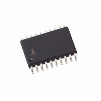
IC DRIVER FULL-BRIDGE 20-SOIC

HIP4020IB

Manufacturer Part Number
HIP4020IB
Description
IC DRIVER FULL-BRIDGE 20-SOIC
Manufacturer
Intersil
Datasheet

Specifications of HIP4020IB

Configuration
H Bridge
Input Type
Inverting and Non-Inverting
Delay Time
2.5µs
Current - Peak
625mA
Number Of Configurations
1
Number Of Outputs
4
Voltage - Supply
3 V ~ 12 V
Operating Temperature
-40°C ~ 85°C
Mounting Type
Surface Mount
Package / Case
20-SOIC (7.5mm Width)
Supply Voltage Min
3V
Supply Voltage Max
12V
Output Current
15mA
Driver Case Style
SOIC
Sink Output Current
15mA
Device Type
Power
Termination Type
SMD
No. Of Pins
20
Rohs Compliant
No
Peak Reflow Compatible (260 C)
No
Lead Free Status / RoHS Status
Contains lead / RoHS non-compliant
High Side Voltage - Max (bootstrap)
-

Available stocks

Company
Part Number
Manufacturer
Quantity
Price
Part Number:
HIP4020IB
Manufacturer:
NS
Quantity:
8
Part Number:
HIP4020IB
Manufacturer:
HARRIS
Quantity:
32
Part Number:
HIP4020IB
Manufacturer:
INTERSIL
Quantity:
20 000
Part Number:
HIP4020IBZ
Manufacturer:
HARRIS
Quantity:
20 000
Part Number:
HIP4020IBZT
Manufacturer:
Intersil
Quantity:
2 000
Half Amp Full Bridge Power Driver for
Small 3V, 5V and 12V DC Motors
In the Functional Block Diagram of the HIP4020, the four
switches and a load are arranged in an H-Configuration so
that the drive voltage from terminals OUTA and OUTB can
be cross-switched to change the direction of current flow in
the load. This is commonly known as 4-quadrant load
control. As shown in the Block Diagram, switches Q1 and Q4
are conducting or in an ON state when current flows from
V
V
with respect to OUTB. Switches Q1 and Q4 are operated
synchronously by the control logic. The control logic
switches Q3 and Q2 to an open or OFF state when Q1 and
Q4 are switched ON. To reverse the current flow in the load,
the switch states are reversed where Q1 and Q4 are OFF
while Q2 and Q3 are ON. Consequently, current then flows
from V
terminal V
potential with respect to OUTA.
Terminals ENA and ENB are ENABLE Inputs for the Logic A
and B Input Controls. The ILF output is an Overcurrent Limit
Fault Flag Output and indicates a fault condition for either
Output A or B or both. The V
Supply reference terminals for the A and B Control Logic
Inputs and ILF Output. While the V
terminal is internally connected to each bridge driver, the
V
independent from V
V
the gate drive circuitry to the NMOS (low-side) output stages
allows controlled level shifting of the output drive relative to
ground.
DD
SSB
SSA
SS
ground reference terminal. The use of level shifters in
through Q1 to the load, and then through Q4 to terminal
; where load terminal OUTA is at a positive potential
and V
DD
through Q3, through the load, and through Q2 to
SSA
SSB
, and load terminal OUTB is then at a positive
Power Supply terminals are separate and
SS
and may be more negative than the
®
DD
1
and V
DD
Data Sheet
SS
positive power supply
are the Power
1-888-INTERSIL or 1-888-468-3774
CAUTION: These devices are sensitive to electrostatic discharge; follow proper IC Handling Procedures.
Features
• Two Independent Controlled Complementary MOS Power
• Split ±Voltage Power Supply Option for Output Drivers
• Load Switching Capabilities to 0.5A
• Single Supply Range +2.5V to +15V
• Low Standby Current
• CMOS/TTL Compatible Input Logic
• Over-Temperature Shutdown Protection
• Overcurrent Limit Protection
• Overcurrent Fault Flag Output
• Direction, Braking and PWM Control
• Pb-Free Plus Anneal Available (RoHS Compliant)
Applications
• DC Motor Driver
• Relay and Solenoid Drivers
• Stepper Motor Controller
• Air Core Gauge Instrument Driver
• Speedometer Displays
• Tachometer Displays
• Remote Power Switch
• Battery Operated Switch Circuits
• Logic and Microcontroller Operated Switch
Ordering Information
NOTE: Intersil Pb-free plus anneal products employ special Pb-free
material sets; molding compounds/die attach materials and 100%
matte tin plate termination finish, which are RoHS compliant and
compatible with both SnPb and Pb-free soldering operations. Intersil
Pb-free products are MSL classified at Pb-free peak reflow
temperatures that meet or exceed the Pb-free requirements of
IPC/JEDEC J STD-020.
HIP4020IB
HIP4020IBZ
(Note)
HIP4020IBZT
(Note)
December 20, 2005
Output Half H-Drivers (Full-Bridge) for Nominal 3V to 12V
Power Supply Operation
NUMBER
PART
All other trademarks mentioned are the property of their respective owners.
|
Intersil (and design) is a registered trademark of Intersil Americas Inc.
HIP4020IB
HIP4020IBZ
HIP4020IBZ
MARKING
Copyright Intersil Americas Inc. 1997, 2005. All Rights Reserved
PART
RANGE (°C)
-40 to 85
-40 to 85
-40 to 85
TEMP.
20 Ld SOIC
20 Ld SOIC
(Pb-free)
20 Ld SOIC
Tape and Reel
(Pb-free)
PACKAGE
HIP4020
FN3976.3
DWG. #
M20.3
M20.3
M20.3
PKG.

Related parts for HIP4020IB

HIP4020IB Summary of contents

Page 1

... All other trademarks mentioned are the property of their respective owners. HIP4020 FN3976.3 PART TEMP. MARKING RANGE (°C) PACKAGE HIP4020IB - SOIC HIP4020IBZ - SOIC (Pb-free) HIP4020IBZ - SOIC Tape and Reel (Pb-free) Intersil (and design registered trademark of Intersil Americas Inc. Copyright Intersil Americas Inc. 1997, 2005. All Rights Reserved PKG ...

Page 2

Pinout HIP4020 (SOIC) TOP VIEW ILF ENB 4 17 OUTB SSB SSA ENA OUTA ...

Page 3

Absolute Maximum Ratings Supply Voltage SSA SSB Neg. Output Supply Voltage SSA SSB DC Logic Input Voltage (Each Input Logic Input Current (Each ...

Page 4

Electrical Specifications T = 25° PARAMETER Thermal Shutdown Response Time OUT Turn-On: Prop Delay Rise Time Turn-Off: Prop Delay Fall Time Pin Descriptions PIN NUMBER SYMBOL 12 Positive Power Supply pins; internally ...

Page 5

B1 B2 BRAKE ON ENB OFF A1 DIRECTION A2 ENA ENABLE FIGURE 1. TYPICAL MOTOR CONTROL APPLICATION CIRCUIT SHOWING DIRECTIONAL AND BRAKING CONTROL TRUTH TABLE SWITCH DRIVER A SWITCH DRIVER B INPUTS OUTPUT INPUTS A1 A2 ENA OUTA B1 B2 ...

Page 6

DIRECTION Input Control terminal. The MOS output transistor pair chosen for conduction is determined by the logic level applied to the DIRECTION control; resulting in either clockwise (CW) or counter-clockwise (CCW) shaft rotation. When the BRAKE terminal is switched high ...

Page 7

Typical Performance Curves 800 0.5Ω 750 700 V 650 600 550 500 450 400 350 300 250 200 150 100 50 0 0.0 0.1 0.2 0.3 0.4 FIGURE 5. TYPICAL CHARACTERISTIC OF THE P-MOSFET OUTPUT DRIVER DRAIN CURRENT vs DRAIN-TO-SOURCE ...

Page 8

Typical Performance Curves 0.65 HIP4020 SPLIT 5V COMMON GROUND 0.60 V SAT 0. 0. 0.45 0.40 0.35 0.30 0.25 0.20 0.15 0.10 0.05 0.00 0 FIGURE 8. TYPICAL CHARACTERISTIC OF SATURATION VOLTAGE vs OUTPUT CURRENT USING ...

Page 9

... Accordingly, the reader is cautioned to verify that data sheets are current before placing orders. Information furnished by Intersil is believed to be accurate and reliable. However, no responsibility is assumed by Intersil or its subsidiaries for its use; nor for any infringements of patents or other rights of third parties which may result from its use ...

Related keywords