VNQ660SP STMicroelectronics, VNQ660SP Datasheet - Page 9
VNQ660SP
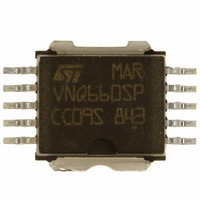
Manufacturer Part Number
VNQ660SP
Description
IC DRIVER QUAD 36V 6A POWERSO-10
Manufacturer
STMicroelectronics
Type
High Sider
Datasheet
1.VNQ660SP.pdf
(26 pages)
Specifications of VNQ660SP
Input Type
Non-Inverting
Number Of Outputs
4
On-state Resistance
40 mOhm
Current - Peak Output
10A
Voltage - Supply
6 V ~ 36 V
Operating Temperature
-40°C ~ 150°C
Mounting Type
Surface Mount
Package / Case
PowerSO-10 Exposed Bottom Pad
Switch Type
High Side
Power Switch Family
VNQ660SP
Power Switch On Resistance
40mOhm
Output Current
6A
Mounting
Surface Mount
Supply Current
6mA
Package Type
PowerSO
Operating Temperature (min)
-40C
Operating Temperature (max)
150C
Operating Temperature Classification
Automotive
Pin Count
10
Power Dissipation
113600W
Lead Free Status / RoHS Status
Contains lead / RoHS non-compliant
Current - Output / Channel
-
Lead Free Status / Rohs Status
Not Compliant
Other names
497-2700-5
Available stocks
Company
Part Number
Manufacturer
Quantity
Price

Part Number:
VNQ660SP
Manufacturer:
ST
Quantity:
20 000
Company:
Part Number:
VNQ660SP13TR
Manufacturer:
ST
Quantity:
714
Part Number:
VNQ660SP13TR
Manufacturer:
INFINEON/英飞凌
Quantity:
20 000


VNQ660SP
Table 8.
Table 9.
Table 10.
Figure 4.
dV
dV
Symbol
Symbol
V
V
V
Symbol
t
t
STAT
V
IN
OUT
OUT
V
SDL
DOL
I(hyst)
C
V
V
t
t
I
I
OL
ICL
d(on)
d(off)
IH
IL
IH
IL
IN
/dt
/dt
(on)
(off)
Status delay
Openload voltage detection threshold
Openload detection delay at turn-off
Input low level voltage
Input low level current
Input high level voltage
Input high level current
Input hysteresis voltage
Input capacitance
Input clamp voltage
OPENLOAD STATUS TIMING
t
Switching (V
Logic inputs
Openload detection
Status timings
DOL
Turn-on delay time
Turn-off delay time
Turn-on voltage slope
Turn-off voltage slope
Parameter
Parameter
Parameter
CC
= 13V; T
R
(see
R
(see
R
(see
R
(see
t
L
L
L
L
SDL
= 13 channels 1,2,3,4
= 13 channels 1,2,3,4
= 13 channels 1,2,3,4
= 13 channels 1,2,3,4
j
Figure
Figure
Figure
Figure
= 25°C)
Test conditions
Test conditions
V
V
I
5)
5)
5)
5)
I
IN
IN
IN
IN
= -1mA
= 1.25V
= 3.25V
= 1mA
Test conditions
(see
See
V
V
V
V
CC
IN
STAT
IN
Figure
Figure 4
= 18V
= 0V
OVERTEMP STATUS TIMING
4)
t
SDL
Min.
Min.
3.25
0.5
1
6
Electrical specifications
Min. Typ. Max.
1.5
Figure 10
Figure 12
Typ.
- 0.7
Typ.
See
See
6.8
40
40
2.5
Max.
1.25
10
40
Max. Unit
300
t
8
3.5
140
20
SDL
70
Unit
Unit
V/µs
V/µs
µA
µA
pF
µs
µs
µs
µs
V
V
V
V
V
V
9/26
Related parts for VNQ660SP
Image
Part Number
Description
Manufacturer
Datasheet
Request
R

Part Number:
Description:
QUAD CHANNEL HIGH SIDE SOLID STATE RELAY
Manufacturer:
STMicroelectronics
Datasheet:
Part Number:
Description:
STMicroelectronics [RIPPLE-CARRY BINARY COUNTER/DIVIDERS]
Manufacturer:
STMicroelectronics
Datasheet:
Part Number:
Description:
STMicroelectronics [LIQUID-CRYSTAL DISPLAY DRIVERS]
Manufacturer:
STMicroelectronics
Datasheet:

Part Number:
Description:
BOARD EVAL FOR MEMS SENSORS
Manufacturer:
STMicroelectronics
Datasheet:
Part Number:
Description:
NPN TRANSISTOR POWER MODULE
Manufacturer:
STMicroelectronics
Datasheet:
Part Number:
Description:
TURBOSWITCH ULTRA-FAST HIGH VOLTAGE DIODE
Manufacturer:
STMicroelectronics
Datasheet:
Part Number:
Description:
Manufacturer:
STMicroelectronics
Datasheet:
Part Number:
Description:
DIODE / SCR MODULE
Manufacturer:
STMicroelectronics
Datasheet:
Part Number:
Description:
DIODE / SCR MODULE
Manufacturer:
STMicroelectronics
Datasheet:
Part Number:
Description:
Search -----> STE16N100
Manufacturer:
STMicroelectronics
Datasheet:
Part Number:
Description:
Search ---> STE53NA50
Manufacturer:
STMicroelectronics
Datasheet:
Part Number:
Description:
NPN Transistor Power Module
Manufacturer:
STMicroelectronics
Datasheet: