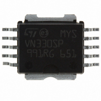
VN330SP-E STMicroelectronics, VN330SP-E Datasheet - Page 4

VN330SP-E
Manufacturer Part Number
VN330SP-E
Description
IC DRIVER QUAD 0.7A POWERSO-10
Manufacturer
STMicroelectronics
Type
High Sider
Specifications of VN330SP-E
Input Type
Non-Inverting
Number Of Outputs
4
On-state Resistance
200 mOhm
Current - Output / Channel
700mA
Current - Peak Output
4A
Voltage - Supply
10 V ~ 36 V
Mounting Type
Surface Mount
Package / Case
PowerSO-10 Exposed Bottom Pad
On Resistance (max)
0.2 Ohms
Mounting Style
SMD/SMT
Supply Current
10 mA
Current, Output
0.7 A @ 85 °C
Package Type
SO-10
Temperature, Ambient, Minimum
-55 °C
Temperature, Range, Operating Ambient
-55 °C
Thermal Resistance, Junction To Ambient
50 °C⁄W
Transistor Type
IGBT
Voltage, Supply
45 V
Switch Type
High Side
Power Switch Family
VN330SP
Power Switch On Resistance
200mOhm
Output Current
700mA
Mounting
Surface Mount
Pin Count
10
Device Type
Relay
Supply Voltage Range
10V To 36V
Driver Case Style
SOIC
No. Of Pins
10
Operating Temperature Range
-40°C To +125°C
Supply Voltage Max
36V
Rohs Compliant
Yes
No. Of Channels
4
Lead Free Status / RoHS Status
Lead free / RoHS Compliant
Operating Temperature
-
Lead Free Status / Rohs Status
Lead free / RoHS Compliant
Other names
497-5052-5
Available stocks
Company
Part Number
Manufacturer
Quantity
Price
Part Number:
VN330SP-E
Manufacturer:
ST
Quantity:
20 000
ELECTRICAL CHARACTERISTICS (continued)
LOGIC INPUT (Per each channel)
Note 1: The input voltage is internally clamped at 32V minimum, it is possible to connect the input pins to an higher voltage via an external
resistor calculate to not exceed 10mA
PROTECTION AND DIAGNOSTICS
(*) Status determination > 100 s after the switching edge.
Note: If INPUT pin is left floating the corrisponding channel will automatically switch off. If GND pin is disconnected, all channels will switch
off provided V
V
Symbol
V
Symbol
V
I
DIAG
I
I
I
V
I(HYST)
SCL
DIAGH
T
LGND
V
OVPK
LOAD
V
V
I
t
V
T
I
USD
LIM
SC
TSD
IN
ICL
OL
IH
IL
R
(*)
(*)
CC
Input low level voltage
Input high level voltage
(see note 1)
Input hysteresis voltage
Input current
Output current in ground
disconnection
Input clamp voltage
(see note 1)
Status voltage output low I
Status clamp voltage
Undervoltage shut down
Low state output voltage
DC Short circuit current
Peak short circuit current
Leakage on diag pin in
high state
Output leakage current
Delay time of current
limiter
Thermal shut down
temperature
Reset temperature
does not exceed 36V.
Parameter
Parameter
V
V
V
I
I
I
I
V
V
V
(see figure 2)
V
V
IN
IN
STAT
DIAG
DIAG
IN
IN
CC
IN
CC
CC
DIAG
CC
=1mA
=-1mA
= 0 to 30V
= 0 to 2V
=V
=V
=24V; R
=24V; V
=10 to 36V; V
=1mA
=-1mA
=5mA (Fault condition)
=24V
ILj
INn
; R
=GND=DIAG=24V; T
LOAD
Test Conditions
Test Conditions
IN
LOAD
=30V; R
10M
<10m
IN
=V
LOAD
IL
<10m
j
=25°C
Min
Min
150
135
3.5
25
32
0.7
32
5
Typ
-0.7
0.5
36
Typ
-0.7
170
155
36
Max
600
25
Max
100
100
2
1.5
2.5
50
1
8
4
VN330SP
Unit
mA
Unit
V
V
V
V
V
°C
°C
V
V
V
V
V
A
A
A
A
A
A
s
4/9
2


