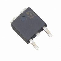
VND5N0713TR STMicroelectronics, VND5N0713TR Datasheet

VND5N0713TR
Specifications of VND5N0713TR
Available stocks
Related parts for VND5N0713TR
VND5N0713TR Summary of contents
Page 1
... Fault feedback can be detected by monitoring the voltage at the input pin. Order codes Tube VND5N07 VND5N07-1 VNP5N07FI VNK5N07FM Rev 3 VND5N07 OMNIFET DPAK IPAK TO-252 TO-251 ISOWATT200 SOT-82FM Tape and reel VND5N0713TR 3 1/24 www.st.com 24 ...
Page 2
Contents Contents 1 Block diagram and pin description . . . . . . . . . . . . . . . . . . . . . . . . . . . . . 5 2 Electrical ...
Page 3
VND5N07 List of tables Table 1. Device summary . . . . . . . . . . . . . . . . . . . . . . . . . . . . . . . . ...
Page 4
List of figures List of figures Figure 1. Block diagram . . . . . . . . . . . . . . . . . . . . . . . . . . . . . . ...
Page 5
VND5N07 1 Block diagram and pin description Figure 1. Block diagram Block diagram and pin description 5/24 ...
Page 6
... These are stress ratings only and operation of the device at these or any other conditions above those indicated in the operating sections of this specification is not implied. Exposure to Absolute maximum rating conditions for extended periods may affect device reliability. Refer also to the STMicroelectronics SURE program and other relevant quality document. Table 2. ...
Page 7
VND5N07 2.3 Electrical characteristics T = 25°C unless otherwise stated. case Table 4. Off Symbol Parameter Drain-Source clamp V CLAMP voltage Drain-Source V CLTH threshold voltage Supply current from I ISS input pin Input-Source reverse V INCL clamp voltage Zero ...
Page 8
Electrical specifications Table 7. Switching Symbol Parameter t Turn-on delay time d(on) t Rise time r t Turn-off delay time d(off) t Fall time f t Turn-on delay time d(on) t Rise time r t Turn-off delay time d(off) t ...
Page 9
VND5N07 Figure 2. Switching time test circuit for resistive load Figure 3. Test circuit for diode recovery times 330Ω FAST OMNIFET DIODE gen I V gen Electrical specifications A L=100uH ...
Page 10
Electrical specifications Figure 4. Unclamped inductive load test circuits Figure 5. Input charge test circuit 10/24 R GEN W GEN VND5N07 ND8003 ...
Page 11
VND5N07 Figure 6. Unclamped inductive waveforms Figure 7. Switching waveforms Electrical specifications 11/24 ...
Page 12
Electrical specifications Figure 8. Thermal impedance for ISOWATT220 Figure 9. Thermal impedance for DPAK / IPAK 12/24 VND5N07 ...
Page 13
VND5N07 2.4 Electrical characteristics curves Figure 10. Source-Drain diode forward characteristics Figure 12. Derating curve Figure 14. Normalized on resistance Vs temperature Electrical specifications Figure 11. Static Drain-Source on resistance Figure 13. Static Drain-Source on resistance vs. input voltage Figure ...
Page 14
Electrical specifications Figure 16. Static Drain-Source on resistance Vs. Id Figure 18. Turn-on current slope (V IN Figure 20. Input voltage Vs. input charge 14/24 Figure 17. Switching time resistive load Figure 19. Turn-on current slope = 10V) Figure 21. ...
Page 15
VND5N07 Figure 22. Turn-off Drain-Source voltage slope Figure 24. Switching time resistive load Figure 25. Step response current limit Figure 26. Output characteristics Electrical specifications Figure 23. Capacitance variations Figure 27. Normalized on resistance Vs. temperature 15/24 ...
Page 16
Electrical specifications Figure 28. Normalized Input threshold voltage Vs. temperature 16/24 Figure 29. Normalized current limit Vs. junction temperature VND5N07 ...
Page 17
VND5N07 3 Protection features During normal operation, the INPUT pin is electrically connected to the gate of the internal power MOSFET. The device then behaves like a standard power MOSFET and can be used as a switch from DC to ...
Page 18
Package and packing information 4 Package and packing information ® 4.1 ECOPACK In order to meet environmental requirements, ST offers these devices in different grades of ECOPACK® packages, depending on their level of environmental compliance. ECOPACK® specifications, grade definitions and ...
Page 19
VND5N07 Table 10. DPAK mechanical data Dim Package weight Package and packing information mm Min. Typ. 2.20 0.90 0.03 0.64 5.20 0.45 ...
Page 20
Package and packing information 4.3 IPAK mechanical data Figure 31. IPAK mechanical data and package outline Table 11. IPAK mechanical data Symbol 20/24 ...
Page 21
VND5N07 4.4 ISOWATT220 mechanical data Figure 32. ISOWATT220 mechanical data and package outline Table 12. ISOWATT220 mechanical data Symbol Package and packing information mm Min. ...
Page 22
Package and packing information 4.5 SOT-82FM mechanical data Figure 33. SOT-82FM mechanical data and package outline Table 13. SOT-82FM mechanical data Symbol 22/24 mm Min. Typ. 2.85 1.47 0.40 ...
Page 23
VND5N07 5 Revision history Table 14. Document revision history Date 09-Sep-2004 17-Dec-2007 11-Dec-2008 Revision 1 Initial release. 2 Stylesheet update. No content change. Document restructured and reformatted. 3 ® Added ECOPACK packages Revision history Changes information. 23/24 ...
Page 24
... Information in this document is provided solely in connection with ST products. STMicroelectronics NV and its subsidiaries (“ST”) reserve the right to make changes, corrections, modifications or improvements, to this document, and the products and services described herein at any time, without notice. All ST products are sold pursuant to ST’s terms and conditions of sale. ...


