VND5N0713TR STMicroelectronics, VND5N0713TR Datasheet - Page 17
VND5N0713TR
Manufacturer Part Number
VND5N0713TR
Description
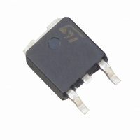
MOSFET N-CH 70V 5A DPAK
Manufacturer
STMicroelectronics
Series
OMNIFET II™r
Type
Low Sider
Datasheet
1.VND5N0713TR.pdf
(24 pages)
Specifications of VND5N0713TR
Input Type
Non-Inverting
Number Of Outputs
1
On-state Resistance
200 mOhm
Current - Peak Output
5A
Mounting Type
Surface Mount
Package / Case
DPak, TO-252 (2 leads+tab), SC-63
Transistor Polarity
N-Channel
Resistance Drain-source Rds (on)
0.2 Ohms
Forward Transconductance Gfs (max / Min)
4 S
Drain-source Breakdown Voltage
70 V
Continuous Drain Current
5 A
Power Dissipation
60 W
Maximum Operating Temperature
+ 150 C
Mounting Style
SMD/SMT
Minimum Operating Temperature
- 40 C
Lead Free Status / RoHS Status
Contains lead / RoHS non-compliant
Voltage - Supply
-
Operating Temperature
-
Current - Output / Channel
-
Lead Free Status / Rohs Status
No
Other names
497-2481-2
Available stocks
Company
Part Number
Manufacturer
Quantity
Price


VND5N07
3
3.1
3.2
3.3
3.4
Protection features
During normal operation, the INPUT pin is electrically connected to the gate of the internal
power MOSFET.
The device then behaves like a standard power MOSFET and can be used as a switch from
DC to 50KHz. The only difference from the user’s standpoint is that a small DC current I
flows into the INPUT pin in order to supply the internal circuitry.
The device integrates:
Overvoltage clamp protection
Internally set at 70V, along with the rugged avalanche characteristics of the Power MOSFET
stage give this device unrivalled ruggedness and energy handling capability. This feature is
mainly important when driving inductive loads.
Linear current limiter circuit
Limits the drain current I
is active, the device operates in the linear region, so power dissipation may exceed the
capability of the heatsink. Both case and junction temperatures increase, and if this phase
lasts long enough, junction temperature may reach the overtemperature threshold T
Overtemperature and short circuit protection
These are based on sensing the chip temperature and are not dependent on the input
voltage. The location of the sensing element on the chip in the power stage area ensures
fast, accurate detection of the junction temperature. Overtemperature cutout occurs at
minimum 150 °C. The device is automatically restarted when the chip temperature falls
below 135 °C .
Status feedback
In the case of an overtemperature fault condition, a Status Feedback is provided through the
Input pin. The internal protection circuit disconnects the input from the gate and connects it
instead to ground via an equivalent resistance of 100 Ω . The failure can be detected by
monitoring the voltage at the Input pin, which will be close to ground potential.
Additional features of this device are ESD protection according to the Human Body model
and the ability to be driven from a TTL Logic circuit (with a small increase in R
D
to I
lim
whatever the INPUT pin voltages. When the current limiter
Protection features
DS(on)
).
jsh.
17/24
ISS
Related parts for VND5N0713TR
Image
Part Number
Description
Manufacturer
Datasheet
Request
R

Part Number:
Description:
MOSFET N-CH 70V 5A DPAK
Manufacturer:
STMicroelectronics
Datasheet:

Part Number:
Description:
MOSFET Power N-Ch 70V 5A OmniFET
Manufacturer:
STMicroelectronics
Datasheet:

Part Number:
Description:
MOSFET OMNIFET 70V 5A IPAK
Manufacturer:
STMicroelectronics
Datasheet:
Part Number:
Description:
MOSFET PWR 70V 5A IPAK
Manufacturer:
STMicroelectronics
Datasheet:
Part Number:
Description:
STMicroelectronics [RIPPLE-CARRY BINARY COUNTER/DIVIDERS]
Manufacturer:
STMicroelectronics
Datasheet:
Part Number:
Description:
STMicroelectronics [LIQUID-CRYSTAL DISPLAY DRIVERS]
Manufacturer:
STMicroelectronics
Datasheet:

Part Number:
Description:
BOARD EVAL FOR MEMS SENSORS
Manufacturer:
STMicroelectronics
Datasheet:
Part Number:
Description:
NPN TRANSISTOR POWER MODULE
Manufacturer:
STMicroelectronics
Datasheet:
Part Number:
Description:
TURBOSWITCH ULTRA-FAST HIGH VOLTAGE DIODE
Manufacturer:
STMicroelectronics
Datasheet:
Part Number:
Description:
Manufacturer:
STMicroelectronics
Datasheet:
Part Number:
Description:
DIODE / SCR MODULE
Manufacturer:
STMicroelectronics
Datasheet:
Part Number:
Description:
DIODE / SCR MODULE
Manufacturer:
STMicroelectronics
Datasheet: