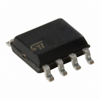
VNS3NV04DTR-E STMicroelectronics, VNS3NV04DTR-E Datasheet

VNS3NV04DTR-E
Specifications of VNS3NV04DTR-E
Available stocks
Related parts for VNS3NV04DTR-E
VNS3NV04DTR-E Summary of contents
Page 1
... Power MOSFETs from 50KHz applications. Built in thermal shutdown, linear current limitation and overvoltage clamp protects the chip in harsh environments. Fault feedback can be detected by monitoring the voltage at the input pin. Tube VNS3NV04D-E Rev 2 VNS3NV04D-E OMNIFET II SO-8 Order codes Tape and Reel VNS3NV04DTR-E 1/21 www.st.com 21 ...
Page 2
Contents Contents 1 Block diagram and pin description . . . . . . . . . . . . . . . . . . . . . . . . . . . . . 5 2 Electrical ...
Page 3
VNS3NV04D-E List of tables Table 1. Device summary . . . . . . . . . . . . . . . . . . . . . . . . . . . . . . . . ...
Page 4
List of figures List of figures Figure 1. Block diagram . . . . . . . . . . . . . . . . . . . . . . . . . . . . . . ...
Page 5
VNS3NV04D-E 1 Block diagram and pin description Figure 1. Block diagram INPUT1 TEMPERATURE Figure 2. Configuration diagram (top view) DRAIN1 OVERVOLTAGE CLAMP GATE CONTROL LINEAR CURRENT OVER LIMITER SOURCE1 1 SOURCE 1 INPUT 1 SOURCE 2 4 INPUT 2 Block ...
Page 6
... These are stress ratings only and operation of the device at these or any other conditions above those indicated in the operating sections of this specification is not implied. Exposure to Absolute maximum rating conditions for extended periods may affect device reliability. Refer also to the STMicroelectronics SURE program and other relevant quality document. Table 2. ...
Page 7
VNS3NV04D-E 2.2 Thermal data Table 3. Thermal data Symbol R Thermal resistance junction-lead (per channel) thj-lead R Thermal resistance junction-ambient thj-amb 1. When mounted on a standard single-sided FR4 board with 50mm to all DRAIN pins of the relative channel ...
Page 8
Electrical specifications Electrical characteristics (continued) (T Table 6. Dynamic Symbol Parameter Forward ( transconductance C Output capacitance OSS Table 7. Switching Symbol Parameter t Turn-on delay time d(on) t Rise Time r t Turn-off delay time d(off) t ...
Page 9
VNS3NV04D-E Table 9. Protections (-40°C < T Symbol Parameter I Drain current limit lim Step response current t dlim limit Overtemperature T jsh shutdown T Overtemperature reset jrs I Fault sink current gf Single pulse E as avalanche energy Figure ...
Page 10
Electrical specifications Figure 5. Test circuit for diode recovery times 220Ω Figure 6. Unclamped inductive load test circuits 10/ FAST OMNIFET DIODE gen I V gen R GEN VNS3NV04D-E A ...
Page 11
VNS3NV04D-E Figure 7. Input charge test circuit Figure 8. Unclamped inductive waveforms V GEN I N Electrical specifications ND8003 11/21 ...
Page 12
Electrical specifications 2.4 Electrical characteristics curves Figure 9. Source-Drain diode forward characteristics Vsd (mV) 1100 1050 Vin= 0V 1000 950 900 850 800 750 700 650 600 Figure 11. Derating curve Figure 13. Static Drain-Source On resistance ...
Page 13
VNS3NV04D-E Figure 15. Static Drain-Source On resistance Vs. Id Rds(on) (mohms) 250 225 Vin= 5V 200 175 150 125 100 0.5 1 Figure 17. Turn On current slope di/dt(A/us) 5 4.5 4 3.5 3 2.5 ...
Page 14
Electrical specifications Figure 21. Turn off Drain-Source voltage slope dv/dt(V/usec) 300 275 250 225 200 175 150 125 100 500 250 Figure 23. Switching time resistive load Figure 24. Switching time resistive load t(usec) 4 ...
Page 15
VNS3NV04D-E Figure 27. Normalized Input threshold voltage Vs. temperature Vinth (V) 2 1.8 Vds= Vin 1 1mA 1.4 1.2 1 0.8 0.6 0.4 0.2 0 -50 -25 0 Figure 29. Step response current limit Tdlim(usec) 13 12.5 12 ...
Page 16
Protection features 3 Protection features During normal operation, the INPUT pin is electrically connected to the gate of the internal power MOSFET through a low impedance path. The device then behaves like a standard power MOSFET and can be used ...
Page 17
VNS3NV04D-E 4 Package and packing information ® 4.1 ECOPACK In order to meet environmental requirements, ST offers these devices in ECOPACK packages. These packages have a Lead-free second-level interconnect. The category of Second-Level Interconnect is marked on the package and ...
Page 18
Package and packing information 4.2 SO-8 Package mechanical data Figure 30. SO-8 package mechanical data & package outline mm DIM. MIN. TYP 0.100 A2 1.250 b 0.280 c 0.170 (1) 4.800 4.900 D E 5.800 6.000 (2) 3.800 ...
Page 19
VNS3NV04D-E 4.3 SO-8 Packing information Figure 31. SO-8 tube shipment (no suffix) Figure 32. SO-8 tape and reel shipment (suffix “TR”) TAPE DIMENSIONS According to Electronic Industries Association (EIA) Standard 481 rev. A, Feb. 1986 Tape width Tape Hole Spacing ...
Page 20
Revision history 5 Revision history Table 10. Document revision history Date 28-Oct-2005 02-Jul-2007 20/21 Revision 1 Initial release. Document reformatted and converted into new ST template. 2 Table 4: Off - I unit corrected DSS VNS3NV04D-E Changes ...
Page 21
... VNS3NV04D-E Information in this document is provided solely in connection with ST products. STMicroelectronics NV and its subsidiaries (“ST”) reserve the right to make changes, corrections, modifications or improvements, to this document, and the products and services described herein at any time, without notice. All ST products are sold pursuant to ST’s terms and conditions of sale. ...


