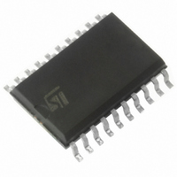
L9333MD STMicroelectronics, L9333MD Datasheet - Page 7

L9333MD
Manufacturer Part Number
L9333MD
Description
IC DRIVER QUAD LOW SIDE SOIC-20
Manufacturer
STMicroelectronics
Type
Low Sider
Datasheet
1.L9333MD-TR.pdf
(13 pages)
Specifications of L9333MD
Input Type
Inverting
Number Of Outputs
4
On-state Resistance
1.7 Ohm
Current - Peak Output
700mA
Voltage - Supply
4.5 V ~ 32 V
Mounting Type
Surface Mount
Package / Case
20-SOIC (7.5mm Width)
Switch Type
Low Side
Power Switch Family
L9333
Input Voltage
-14 to 45V
Output Current
15A
Mounting
Surface Mount
Package Type
SO
Operating Temperature (min)
-40C
Operating Temperature (max)
150C
Operating Temperature Classification
Automotive
Pin Count
20
Lead Free Status / RoHS Status
Lead free / RoHS Compliant
Operating Temperature
-
Current - Output / Channel
-
Lead Free Status / Rohs Status
Compliant
Available stocks
Company
Part Number
Manufacturer
Quantity
Price
Part Number:
L9333MD
Manufacturer:
ST
Quantity:
20 000
Part Number:
L9333MD-TR
Manufacturer:
ST
Quantity:
20 000
FUNCTIONAL DESCRIPTION
The L9333 is a quad low side driver for lines, lamps or inductive loads in automotive and industrial applications.
The logic input levels are 3.3V CMOS compatible. This allows the device to be driven directly by a microcon-
troller. For the noise immunity, all input thresholds have a hysteresis of typ. 100mV. Each input (IN, EN and
PRG) is protected to withstand voltages from -14V to 45V. The device is activated with a 'high' signal on ENable.
ENable 'low' switches the device into the sleep mode. In this mode the quiescent current is typically less than
2µA. A high signal on PRoGramming input changes the signal transfer polarity from noninverting to the inverting
mode. This pin can be connected either to V
PRG and EN pin is low. For packaged applications it is still recommended to connect all input pins to ground
respective VS to avoid EMC influence. The forced condition leads to a mode change if the PRG pin was high
before the interruption. Independent of the PRoGramming input, the OUTput switches off, if the signal INput pin
is not connected. This function is verified using a leakage current of 5µA (sink for PRG=high; source for
PRG=low) during circuit test.
Each output driver has a current limitation of min 0.4A and an independent thermal shut-down. The thermal
shut-down deactivates that output, which exceeds temperature switch off level. When the junction temperature
decreases 20K below this temperature threshold the output will be activated again. This 20K is the hysteresis
of the thermal shutdown function. The Gates, of the output DMOS transistors are charged and discharged with
a current source. Therefore the output slope is limited. This reduces the electromagnetic radiation. For induc-
tive loads an output voltage clamp of typically 52V is implemented.
The DIAGnostic is an open drain output. The logic status depends on the PRoGramming pin. If the PRG pin is
'low' the DIAG output becomes low, if the device works correctly. At thermal shut-down of one channel or if the
ground is disconnected the DIAGnostic output becomes high. If the PRG pin is 'high' this output is switched off
at normal function and switched on at overtemperature. For the fault condition of interrupted ground, the poten-
tial of VS and Diagnostic should be equal.
DIAGNOSTIC TABLE
X = not relevant
* selective for each channel at overtemperature
Normal function
Overtemperature,
disconnected ground or
supply voltage
Overtemperature
Pins
EN
H
H
H
H
H
H
L
S
or GND. If these pins are not connected, the forced status of the
PRG
H
H
H
X
L
L
L
IN
H
H
X
L
X
X
L
H (off)
H(off)
H (off)
H (off)
H (off)
L (on)
L (on)
OUT
*
*
H (off)
H (off)
H (off)
H (off)
L (on)
L (on)
DIAG
L(on)
L9333
7/13


