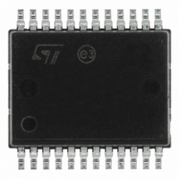
VNQ5050KTR-E STMicroelectronics, VNQ5050KTR-E Datasheet - Page 7

VNQ5050KTR-E
Manufacturer Part Number
VNQ5050KTR-E
Description
IC DRIVER HISIDE QUAD POWERSSO24
Manufacturer
STMicroelectronics
Type
High Sider
Datasheet
1.VNQ5050KTR-E.pdf
(31 pages)
Specifications of VNQ5050KTR-E
Input Type
Non-Inverting
Number Of Outputs
4
On-state Resistance
50 mOhm
Current - Peak Output
19A
Voltage - Supply
4.5 V ~ 36 V
Operating Temperature
-40°C ~ 150°C
Mounting Type
Surface Mount
Package / Case
PowerSSO-24
Number Of Drivers
4
Driver Configuration
Non-Inverting
Driver Type
High Side
Input Logic Level
CMOS
Operating Supply Voltage (max)
36V
Peak Output Current
12A
Operating Supply Voltage (min)
4.5V
Operating Supply Voltage (typ)
13V
Turn Off Delay Time
40us
Turn On Delay Time (max)
15us
Operating Temp Range
-40C to 150C
Operating Temperature Classification
Automotive
Mounting
Surface Mount
Pin Count
24
Package Type
PowerSSO
Supply Voltage (min)
4.5 V
Supply Current
14 mA
Maximum Operating Temperature
+ 150 C
Mounting Style
SMD/SMT
Maximum Turn-off Delay Time
40000 ns
Maximum Turn-on Delay Time
15000 ns
Minimum Operating Temperature
- 40 C
Lead Free Status / RoHS Status
Lead free / RoHS Compliant
Current - Output / Channel
-
Lead Free Status / Rohs Status
Compliant
Available stocks
Company
Part Number
Manufacturer
Quantity
Price
Company:
Part Number:
VNQ5050KTR-E
Manufacturer:
st
Quantity:
5 000
Company:
Part Number:
VNQ5050KTR-E
Manufacturer:
STM
Quantity:
294
Part Number:
VNQ5050KTR-E
Manufacturer:
ST
Quantity:
20 000
VNQ5050K-E
2
Note:
2.1
Electrical specifications
Figure 3.
V
Absolute maximum ratings
Stressing the device above the ratings listed in the “Absolute maximum ratings” tables may
cause permanent damage to the device. These are stress ratings only and operation of the
device at these or any other conditions above those indicated in the Operating sections of
this specification is not implied. Exposure to the conditions in this section for extended
periods may affect device reliability. Refer also to the STMicroelectronics SURE Program
and other relevant quality documents.
Table 4.
I
Symbol
Fn
STAT_DIS
- I
- I
- V
E
I
I
V
STAT
OUT
I
MAX
GND
OUT
= V
CC
IN
CC
OUTn
DC supply voltage
Reverse DC supply voltage
DC reverse ground pin current
DC output current
Reverse DC output current
DC input current
DC status current
DC status disable current
Maximum switching energy (single pulse)
(L=3 mH; R
I
V
OUT
SD
Current and voltage conventions
Absolute maximum ratings
- V
= I
V
CC
INn
limL
during reverse battery condition
(typ.))
L
=0Ω; V
I
I
SD
INn
bat
Doc ID 10864 Rev 6
=13.5V; T
STAT_DIS
INPUTn
Parameter
jstart
GND
=150ºC;
I
GND
OUTPUTn
STATUSn
V
CC
I
OUTn
I
STATn
Electrical specifications
V
Internally limited
STATn
+10 / -1
V
Value
+10/-1
+10/-1
200
104
OUTn
0.3
41
15
I
S
V
CC
Unit
mA
mA
mA
mA
mJ
V
V
A
A
7/31


