L298P STMicroelectronics, L298P Datasheet - Page 3
L298P
Manufacturer Part Number
L298P
Description
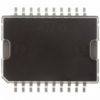
IC DRIVER FULL DUAL 20POWERRSOIC
Manufacturer
STMicroelectronics
Type
H Bridger
Datasheet
1.L298N.pdf
(13 pages)
Specifications of L298P
Input Type
Non-Inverting
Number Of Outputs
4
Current - Output / Channel
2A
Current - Peak Output
3A
Voltage - Supply
4.5 V ~ 46 V
Operating Temperature
-25°C ~ 130°C
Mounting Type
Surface Mount
Package / Case
PowerSO-20 Exposed Bottom Pad
Operating Temperature Classification
Commercial
Package Type
PowerSO
Operating Supply Voltage (min)
4.5V
Operating Supply Voltage (typ)
42V
Operating Supply Voltage (max)
46V
Operating Supply Voltage
4.8 V to 46 V
Mounting Style
SMD/SMT
Lead Free Status / RoHS Status
Lead free / RoHS Compliant
On-state Resistance
-
Lead Free Status / Rohs Status
Compliant
Other names
497-1396-5
Available stocks
Company
Part Number
Manufacturer
Quantity
Price
Company:

Part Number:
L298P
Manufacturer:
STMicroelectronics
Quantity:
456
Part Number:
L298P
Manufacturer:
ST
Quantity:
20 000
Part Number:
L298P013TR
Manufacturer:
ST
Quantity:
20 000
Part Number:
L298P031TR
Manufacturer:
ST
Quantity:
20 000


PIN FUNCTIONS (refer to the block diagram)
ELECTRICAL CHARACTERISTICS (V
Symbol
V
V
V
V
I
I
V
en
CEsat (H)
CEsat (L)
MW.15
en
V
en
en
V
10; 12
13; 14
V
I
V
CEsat
V
I
sens
I
I
1;15
6;11
SS
iH
SS
S
iL
= H
2;3
5;7
iH
= L
S
iL
= H
= L
4
8
9
–
Supply Voltage (pin 4)
Logic Supply Voltage (pin 9)
Quiescent Supply Current (pin 4)
Quiescent Current from V
Input Low Voltage
(pins 5, 7, 10, 12)
Input High Voltage
(pins 5, 7, 10, 12)
Low Voltage Input Current
(pins 5, 7, 10, 12)
High Voltage Input Current
(pins 5, 7, 10, 12)
Enable Low Voltage (pins 6, 11)
Enable High Voltage (pins 6, 11)
Low Voltage Enable Current
(pins 6, 11)
High Voltage Enable Current
(pins 6, 11)
Source Saturation Voltage
Sink Saturation Voltage
Total Drop
Sensing Voltage (pins 1, 15)
PowerSO
1,10,11,20
13;15
16;17
2;19
8;14
3;18
4;5
7;9
12
6
Parameter
Enable A; Enable B
Sense A; Sense B
Input 1; Input 2
Input 3; Input 4
Out 1; Out 2
Out 3; Out 4
Name
GND
SS
VSS
N.C.
V
S
(pin 9) V
S
= 42V; V
Operative Condition
V
V
V
V
Vi = H
V
V
I
I
I
I
I
I
L
L
L
L
L
L
en
en
en
en
i
en
en
= 1A
= 2A
= 1A
= 2A
= 1A
= 2A
= L
Between this pin and ground is connected the sense resistor to
control the current of the load.
Outputs of the Bridge A; the current that flows through the load
connected between these two pins is monitored at pin 1.
Supply Voltage for the Power Output Stages.
A non-inductive 100nF capacitor must be connected between this
pin and ground.
TTL Compatible Inputs of the Bridge A.
TTL Compatible Enable Input: the L state disables the bridge A
(enable A) and/or the bridge B (enable B).
Ground.
Supply Voltage for the Logic Blocks. A100nF capacitor must be
connected between this pin and ground.
TTL Compatible Inputs of the Bridge B.
Outputs of the Bridge B. The current that flows through the load
connected between these two pins is monitored at pin 15.
Not Connected
= H; I
= L
= H; I
= L
= L
= H
Test Conditions
V
SS
(5)
(5)
(5)
(5)
V
SS
L
L
SS
= 5V, T
= 0
= 0
–0.6V
–0.6V
j
= 25 C; unless otherwise specified)
V
V
V
V
V
V
i
i
i
i
i
i
= L
= L
= H
= H
= X
= X
Function
V
–1 (1)
Min.
IH
–0.3
–0.3
0.95
0.85
1.80
4.5
2.3
2.3
+2.5
Typ.
1.35
1.2
1.7
13
50
24
30
30
5
7
2
Max.
VSS
100
–10
100
V
–10
1.5
1.5
1.7
2.7
1.6
2.3
3.2
4.9
46
22
70
36
12
7
4
6
2
SS
L298
Unit
mA
mA
mA
mA
mA
mA
V
V
V
V
V
V
V
V
V
V
V
V
V
A
A
A
A
3/13
Related parts for L298P
Image
Part Number
Description
Manufacturer
Datasheet
Request
R

Part Number:
Description:
DUAL FULL-BRIDGE DRIVER
Manufacturer:
STMicroelectronics
Datasheet:
Part Number:
Description:
STMicroelectronics [RIPPLE-CARRY BINARY COUNTER/DIVIDERS]
Manufacturer:
STMicroelectronics
Datasheet:
Part Number:
Description:
STMicroelectronics [LIQUID-CRYSTAL DISPLAY DRIVERS]
Manufacturer:
STMicroelectronics
Datasheet:

Part Number:
Description:
BOARD EVAL FOR MEMS SENSORS
Manufacturer:
STMicroelectronics
Datasheet:
Part Number:
Description:
NPN TRANSISTOR POWER MODULE
Manufacturer:
STMicroelectronics
Datasheet:
Part Number:
Description:
TURBOSWITCH ULTRA-FAST HIGH VOLTAGE DIODE
Manufacturer:
STMicroelectronics
Datasheet:
Part Number:
Description:
Manufacturer:
STMicroelectronics
Datasheet:
Part Number:
Description:
DIODE / SCR MODULE
Manufacturer:
STMicroelectronics
Datasheet:
Part Number:
Description:
DIODE / SCR MODULE
Manufacturer:
STMicroelectronics
Datasheet:
Part Number:
Description:
Search -----> STE16N100
Manufacturer:
STMicroelectronics
Datasheet:
Part Number:
Description:
Search ---> STE53NA50
Manufacturer:
STMicroelectronics
Datasheet:
Part Number:
Description:
NPN Transistor Power Module
Manufacturer:
STMicroelectronics
Datasheet: