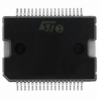
L6206PD STMicroelectronics, L6206PD Datasheet - Page 13

L6206PD
Manufacturer Part Number
L6206PD
Description
IC DRIVER DUAL FULL 36-PWRSOIC
Manufacturer
STMicroelectronics
Type
H Bridger
Datasheet
1.L6206N.pdf
(23 pages)
Specifications of L6206PD
Input Type
Non-Inverting
Number Of Outputs
4
On-state Resistance
300 mOhm
Current - Output / Channel
2.8A
Current - Peak Output
5.6A
Voltage - Supply
8 V ~ 52 V
Operating Temperature
-25°C ~ 125°C
Mounting Type
Surface Mount
Package / Case
36-PowerSOIC
Operating Supply Voltage
48 V
Mounting Style
SMD/SMT
For Use With
497-4135 - EVAL BOARD FOR L6206 SERIES
Lead Free Status / RoHS Status
Lead free / RoHS Compliant
Other names
497-5341-5
L6206PD
L6206PD
Available stocks
Company
Part Number
Manufacturer
Quantity
Price
Company:
Part Number:
L6206PD
Manufacturer:
STMicroelectronics
Quantity:
182
Company:
Part Number:
L6206PD013TR
Manufacturer:
TI
Quantity:
2 001
Part Number:
L6206PD013TR
Manufacturer:
ST
Quantity:
20 000
APPLICATION INFORMATION
A typical application using L6206 is shown in Fig. 12. Typical component values for the application are shown
in Table 2. A high quality ceramic capacitor in the range of 100 to 200 nF should be placed between the power
pins (VS
reduce high frequency transients generated by the switching. The capacitors connected from the EN
and EN
over current is detected (see Overcurrent Protection). The two current sources (SENSE
be connected to Power Ground with a trace length as short as possible in the layout. To increase noise immu-
nity, unused logic pins are best connected to 5V (High Logic Level) or GND (Low Logic Level) (see pin descrip-
tion). It is recommended to keep Power Ground and Signal Ground separated on PCB.
Table 2. Component Values for Typical Application
Figure 12. Typical Application
C
C
C
C
C
C
C
8-52V
1
2
BOOT
P
ENA
ENB
REF
VS
+
GROUND
-
DC
POWER
B
GROUND
SIGNAL
A
/OCD
and VS
C
1
B
nodes to ground set the shut down time for the Brgidge A and Bridge B respectively when an
B
) and ground near the L6206 to improve the high frequency filtering on the power supply and
C
2
C
BOOT
D
1
100uF
100nF
220nF
LOAD
LOAD
5.6nF
5.6nF
10nF
68nF
D
2
A
B
R
P
SENSE
SENSE
VBOOT
C
OUT1
OUT2
OUT1
OUT2
P
GND
GND
GND
GND
VCP
VS
VS
A
B
A
B
A
A
B
B
20
17
22
15
3
10
5
21
8
16
18
19
6
7
D
D
R
R
R
R
R
1
2
CLA
CLB
ENA
ENB
P
D02IN1344
23
14
11
12
24
13
4
9
1
2
OCD
EN
OCD
EN
IN1
IN2
IN1
IN2
PROGCL
PROGCL
A
B
B
B
A
A
A
B
A
and SENSE
A
B
1N4148
1N4148
C
C
R
R
100k
100k
100
ENA
ENB
CLA
CLB
5K
5K
R
R
ENA
ENB
IN1
IN2
IN1
IN2
B
B
B
A
A
A
) should
L6206
/OCD
EN
EN
13/23
A
B
A


