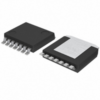
BD6230HFP-TR Rohm Semiconductor, BD6230HFP-TR Datasheet - Page 14

BD6230HFP-TR
Manufacturer Part Number
BD6230HFP-TR
Description
IC H-BRIDGE DVR 36V 1CH .5A HRP7
Manufacturer
Rohm Semiconductor
Series
-r
Type
Half Bridge Driverr
Datasheet
1.BD6230HFP-TR.pdf
(17 pages)
Specifications of BD6230HFP-TR
Applications
DC Motor Driver
Number Of Outputs
1
Current - Output
500mA
Voltage - Supply
6 V ~ 32 V
Operating Temperature
-40°C ~ 85°C
Mounting Type
Surface Mount
Package / Case
HRP-7
Evaluation Tools
-
Voltage - Load
-
Product
H-Bridge Drivers
Supply Voltage (max)
36 V
Supply Voltage (min)
6 V
Supply Current
1.3 mA
Maximum Power Dissipation
1.4 W
Maximum Operating Temperature
+ 85 C
Mounting Style
SMD/SMT
Bridge Type
H-bridge
Minimum Operating Temperature
- 40 C
Number Of Drivers
1
Output Current
0.5 A
Operating Supply Voltage
6 V to 32 V
Lead Free Status / RoHS Status
Lead free / RoHS Compliant
Voltage - Load
-
Lead Free Status / Rohs Status
Lead free / RoHS Compliant
Available stocks
Company
Part Number
Manufacturer
Quantity
Price
Company:
Part Number:
BD6230HFP-TR
Manufacturer:
ROHM Semiconductor
Quantity:
1 937
Ordering part number
○
BD6230, BD6231, BD6232, BD6235, BD6236, BD6237
c
www.rohm.com
2009 ROHM Co., Ltd. All rights reserved.
11) Testing on application boards
12) Switching noise
13) Regarding the input pin of the IC
When testing the IC on an application board, connecting a capacitor to a low impedance pin subjects the IC to stress.
Therefore, always discharge capacitors after each process or step. Always turn the IC's power supply off before
connecting it to or removing it from the test setup during the inspection process. Ground the IC during assembly steps
as an antistatic measure. Use similar precaution when transporting or storing the IC.
When the operation mode is in PWM control or VREF control, PWM switching noise may effects to the control input
pins and cause IC malfunctions. In this case, insert a pulled down resistor (10kΩ is recommended) between each
control input pin and ground.
This monolithic IC contains P+ isolation and P substrate layers between adjacent elements, in order to keep them
isolated. P-N junctions are formed at the intersection of these P layers with the N layers of other elements, creating a
parasitic diode or transistor. For example, the relation between each potential is as follows:
Parasitic diodes inevitably occur in the structure of the IC. The operation of parasitic diodes can result in mutual
interference among circuits, as well as operating malfunctions and physical damage. Therefore, do not use methods by
which parasitic diodes operate, such as applying a voltage lower than the GND (P substrate) voltage to an input pin.
ROHM part
number
When GND > Pin A and GND > Pin B, the P-N junction operates as a parasitic diode.
When GND > Pin B, the P-N junction operates as a parasitic transistor.
Parasitic element
B
Pin A
N
P
+
D
N
Type
1X: 7V max.
2X: 18V max.
3X: 36V max.
X0: 1ch/0.5A X5:
2ch/0.5A
X1: 1ch/1A
X2 1 h/2A
GND
6
P
P substrate
P
+
2
Resistor
N
X6: 2ch/1A
X7 2 h/2A
Pin A
3
Appendix: Example of monolithic IC structure
2
Parasitic
element
Package
F: SOP8
FP: HSOP25
FM: HSOP-M28
HFP: HRP7
14/16
F
Parasitic element
Pin B
N
P
P
+
C
-
B
N
E
GND
P
Transistor (NPN)
P substrate
Packaging spec.
E2: Embossed taping
TR: Embossed taping
E
P
+
N
(SOP8/HSOP25/HSOP-M28)
(HRP7)
GND
2
Other adjacent elements
Pin B
2009.08 - Rev.C
B
Technical Note
C
E
GND
Parasitic
element


