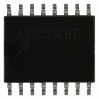
A3953SLBTR-T Allegro Microsystems Inc, A3953SLBTR-T Datasheet - Page 8

A3953SLBTR-T
Manufacturer Part Number
A3953SLBTR-T
Description
IC MOTOR DRIVER PWM FULL 16-SOIC
Manufacturer
Allegro Microsystems Inc
Datasheet
1.A3953SLBTR-T.pdf
(12 pages)
Specifications of A3953SLBTR-T
Applications
PWM Motor Driver
Number Of Outputs
1
Current - Output
±1.3A
Voltage - Load
3 V ~ 50 V
Voltage - Supply
3 V ~ 5.5 V
Operating Temperature
-20°C ~ 85°C
Mounting Type
Surface Mount
Package / Case
16-SOIC (0.300", 7.5mm Width)
Motor Type
Full Bridge
No. Of Outputs
1
Output Current
1.3A
Output Voltage
50V
Supply Voltage Range
3V To 5.5V
Driver Case Style
SOIC
No. Of Pins
16
Lead Free Status / RoHS Status
Lead free / RoHS Compliant
Other names
620-1133-2
A3953SLBTR-T
A3953SLBTR-T
Available stocks
Company
Part Number
Manufacturer
Quantity
Price
Part Number:
A3953SLBTR-T
Manufacturer:
ALLEGRO/雅丽高
Quantity:
20 000
A3953
During braking, when the MODE input is high, the peak current
limit can be approximated by:
CAUTION: Because the kinetic energy stored in the motor
and load inertia is being converted into current, which charges
the V
decoupling capacitance), care must be taken to ensure the
capacitance is sufficient to absorb the energy without exceeding
the voltage rating of any devices connected to the motor supply.
Brake Operation - MODE Input Low.
with the MODE input low, the internal current-control circuitry
is disabled. Therefore, care should be taken to ensure that the
motor’s current does not exceed the ratings of the device. The
braking current can be measured by using an oscilloscope with
a current probe connected to one of the motor’s leads, or if the
back-EMF voltage of the motor is known, approximated by:
RC Fixed Off-Time.
circuitry uses a one shot to control the time the driver(s)
remain(s) off. The one-shot time, t
determined by the selection of an external resistor (R
capacitor (C
to ground. The fixed off-time, over a range of values of C
pF to 1500 pF and R
The operation of the circuit is as follows: when the PWM latch is
reset by the current comparator, the voltage on the RC terminal
will begin to decay from approximately 0.60V
voltage on the RC terminal reaches approximately 0.22V
PWM latch is set, thereby enabling the driver(s).
RC Blanking.
the PWM control circuit, the C
blanking time. This function blanks the output of the comparator
when the outputs are switched by the internal current-control
circuitry (or by the PHASE, BRAKE, or ENABLE inputs).
BB
supply bulk capacitance (power supply output and
T
) connected in parallel from the RC timing terminal
I
PEAK BRAKE ML
In addition to determining the fixed off-time of
I
TRIP BRAKE MH
T
= 12 kΩ to 100 kΩ, is approximated by:
The internal PWM current-control
t
OFF
≈ R
≈
T
component sets the comparator
≈
T
OFF
x C
V
BEMF
(fixed off-time), is
T
R
V
LOAD
R
REF
S
– 1V
CC
During braking,
. When the
T
) and
CC
T
= 470
, the
Full-Bridge PWM Motor Driver
The comparator output is blanked to prevent false over-current
detections due to reverse recovery currents of the clamp diodes,
and/or switching transients related to distributed capacitance in
the load.
During internal PWM operation, at the end of the t
comparator’s output is blanked and C
from approximately 0.22V
approximately 1 mA. The comparator output remains blanked
until the voltage on C
When a transition of the PHASE input occurs, C
to near ground during the crossover delay time (the crossover
delay time is present to prevent simultaneous conduction of
the source and sink drivers). After the crossover delay, C
charged by an internal current source of approximately 1 mA.
The comparator output remains blanked until the voltage on C
reaches approximately 0.60V
When the device is disabled, via the ENABLE input, C
discharged to near ground. When the device is re-enabled, C
charged by an internal current source of approximately 1 mA.
The comparator output remains blanked until the voltage on C
reaches approximately 0.60V
For 3.3 V operation, the minimum recommended value
for C
recommended value for C
ensure that the blanking time is sufficient to avoid false trips
of the comparator under normal operating conditions. For
optimal regulation of the load current, the above values for C
are recommended and the value of R
t
below.
LOAD CURRENT REGULATION
WITH INTERNAL PWM
CURRENT-CONTROL CIRCUITRY
When the device is operating in slow current-decay mode,
there is a limit to the lowest level that the PWM current-
control circuitry can regulate load current. The limitation is the
minimum duty cycle, which is a function of the user-selected
OFF
. For more information regarding load current regulation, see
T
is 680 pF ± 5 %. For 5.0 V operation, the minimum
T
reaches approximately 0.60V
115 Northeast Cutoff
1.508.853.5000; www.allegromicro.com
Allegro MicroSystems, Inc.
Worcester, Massachusetts 01615-0036 U.S.A.
CC
T
CC
CC
is 470 pF ± 5%. These values
by an internal current source of
.
.
T
T
can be sized to determine
begins to be charged
T
is discharged
OFF
CC
time, the
.
T
T
is
is
T
T
is
T
T
7


