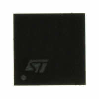
L6228QTR STMicroelectronics, L6228QTR Datasheet - Page 11

L6228QTR
Manufacturer Part Number
L6228QTR
Description
IC DVR BIPO STEP MOTOR 32-VFQFPN
Manufacturer
STMicroelectronics
Type
Bipolar Stepper Motor Driverr
Datasheet
1.L6228QTR.pdf
(32 pages)
Specifications of L6228QTR
Applications
Stepper Motor Driver
Number Of Outputs
1
Current - Output
1.4A
Voltage - Supply
8 V ~ 52 V
Operating Temperature
-25°C ~ 125°C
Mounting Type
Surface Mount
Package / Case
32-VFQFN, 32-VFQFPN
Product
Stepper Motor Controllers / Drivers
Operating Supply Voltage
48 V
For Use With
497-6818 - EVAL BOARD FOR L6228Q
Lead Free Status / RoHS Status
Lead free / RoHS Compliant
Voltage - Load
-
Lead Free Status / Rohs Status
Lead free / RoHS Compliant
Other names
497-6864-2
L6228QTR
L6228QTR
Available stocks
Company
Part Number
Manufacturer
Quantity
Price
Part Number:
L6228QTR
Manufacturer:
ST
Quantity:
20 000
L6228Q
4
4.1
Circuit description
Power stages and charge pump
The L6228Q integrates two independent power MOS full bridges. Each power MOS has an
R
patterns are generated by the PWM Current Controller and the Phase Sequence Generator
(see below). Cross conduction protection is achieved using a dead time (t
value) between the switch off and switch on of two power MOSFETs in one leg of a bridge.
Pins VS
operates with a supply voltage in the range from 8 V to 52 V. It has to be noticed that the
R
12 V.
Using N-channel power MOS for the upper transistors in the bridge requires a gate drive
voltage above the power supply voltage. The bootstrapped supply voltage V
through an internal Oscillator and few external components to realize a charge pump circuit
as shown in
10V amplitude. Recommended values/part numbers for the charge pump circuit are shown
in
Table 6.
Figure 8.
DS(on)
DS(on)
Table
= 0.73 Ω (typical value @ 25 °C), with intrinsic fast freewheeling diode. Switching
increases of some percents when the supply voltage is in the range from 8 V to
A
6.
and VS
Figure
Charge pump external components values
Charge pump circuit
Component
C
B
BOOT
C
D1
D2
must be connected together to the supply voltage V
8. The oscillator output (VCP) is a square wave at 600 kHz (typical) with
P
VCP
Doc ID 14321 Rev 4
D1
C
P
D2
VBOO T
C
BOO T
VS
A
VS
B
D01IN1328
1N4148
1N4148
220 nF
Value
10 nF
V
S
S
Circuit description
. The device
DT
= 1 μs typical
BOOT
is obtained
11/32


