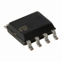
L6562DTR STMicroelectronics, L6562DTR Datasheet - Page 4

L6562DTR
Manufacturer Part Number
L6562DTR
Description
IC PFC CTRLR TRANSITION 8SOIC
Manufacturer
STMicroelectronics
Datasheet
1.L6562N.pdf
(16 pages)
Specifications of L6562DTR
Mode
Discontinuous (Transition)
Frequency - Switching
1MHz
Current - Startup
40µA
Voltage - Supply
10.3 V ~ 22 V
Operating Temperature
-25°C ~ 125°C
Mounting Type
Surface Mount
Package / Case
8-SOIC (3.9mm Width)
Start-up Supply Current
40uA
Operating Supply Voltage (min)
10.3V
Operating Supply Voltage (max)
22V
Operating Temp Range
-40C to 150C
Operating Temperature Classification
Automotive
Package Type
SOIC
Pin Count
8
Mounting
Surface Mount
Maximum Operating Temperature
+ 150 C
Mounting Style
SMD/SMT
Minimum Operating Temperature
- 40 C
For Use With
497-8406 - BOARD STF20NM50FD/STF7LITE39BF2497-8249 - BOARD EVAL FOR L6562AX497-8248 - BOARD EVAL FOR L6562AX
Lead Free Status / RoHS Status
Lead free / RoHS Compliant
Other names
497-3366-2
497-3366-2
497-4583-2
E-L6562DTR
497-3366-2
497-4583-2
E-L6562DTR
Available stocks
Company
Part Number
Manufacturer
Quantity
Price
Company:
Part Number:
L6562DTR
Manufacturer:
ST
Quantity:
5 000
Part Number:
L6562DTR
Manufacturer:
ST
Quantity:
20 000
Part Number:
L6562DTR-75TLF
Manufacturer:
ST
Quantity:
20 000
L6562
Table 5. Electrical Characteristics (continued)
(T
(1)
(2)
(3)
4/16
CURRENT SENSE COMPARATOR
V
ZERO CURRENT DETECTOR
STARTER
OUTPUT OVERVOLTAGE
GATE DRIVER
Symbol
V
V
V
I
V
V
I
V
V
I
t
j
CS clamp
V
V
I
t
ZCDsnk
ZCDsrc
ZCDres
CSoffset
I
START
COMP
Oclamp
d(H-L)
ZCDdis
I
V
= -25 to 125°C, V
ZCDb
ZCDen
Hys
V
COMP
GB
ZCDH
I
ZCDL
ZCDA
ZCDT
OVP
G
CS
All parameters are in tracking
The multiplier output is given by:
Parameters guaranteed by design, functionality tested in production.
OH
t
t
OL
f
r
v
Voltage Gain
Gain-Bandwidth Product
Source Current
Sink Current
Upper Clamp Voltage
Lower Clamp Voltage
Input Bias Current
Delay to Outpu
Current sense reference clamp
Current sense offset
Upper Clamp Voltage
Lower Clamp Voltage
Arming Voltage
(positive-going edge)
Triggering Voltage
(negative-going edge)
Input Bias Current
Source Current Capability
Sink Current Capability
Disable threshold
Restart threshold
Restart Current after Disable
Start Timer period
Dynamic OVP triggering current
Hysteresis
Static OVP threshold
Dropout Voltage
Voltage Fall Time
Voltage Rise Time
Output clamp voltage
UVLO saturation
Parameter
CC
t
= 12, C
V
cs
O
=
= 1 nF; unless otherwise specified)
K V
⋅
MUL T
Open loop
V
V
I
I
V
V
V
V
I
I
(3)
(3)
V
(3)
(1)
I
I
I
I
V
⋅
SOURCE
SINK
ZCD
ZCD
GDsource
GDsource
GDsink
GDsource
(
COMP
COMP
CS
COMP
MULT
MULT
ZCD
CC
V
CO MP
= 0
= 0 to V
= 2.5 mA
= -2.5 mA
= 0.5 mA
= 1 to 4.5 V
= 0
= 2.5V
= 200 mA
= 4V, V
= 4V, V
= Upper clamp
= 0.5 mA
–
= 20 mA
= 200 mA
= 5mA; Vcc = 20V
Test Condition
2.5
CCon
)
INV
INV
(1)
, I
= 2.4 V
= 2.6 V
sink
=10mA
Min.
-2.5
150
2.5
5.3
2.1
1.6
5.0
0.3
2.5
2.1
60
30
75
35
10
-2
Typ.
2.25
0.65
2.25
-3.5
200
200
130
4.5
5.7
1.7
5.7
2.1
1.6
2.5
0.9
80
30
75
40
30
30
40
12
1
5
2
2
Max.
-5.5
350
250
350
300
2.4
1.8
6.5
2.4
2.6
1.9
1.1
45
70
80
15
-5
-1
6
1
3
MHz
Unit
mA
mA
mV
mA
mA
mV
mV
dB
µA
µA
µA
µA
µA
ns
µs
ns
ns
V
V
V
V
V
V
V
V
V
V
V
V


