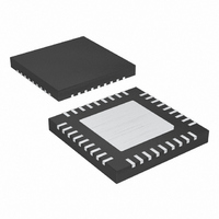
MAX8798ETX+ Maxim Integrated Products, MAX8798ETX+ Datasheet - Page 20

MAX8798ETX+
Manufacturer Part Number
MAX8798ETX+
Description
IC INTERNAL-SW BOOST REG 36-TQFN
Manufacturer
Maxim Integrated Products
Datasheet
1.MAX8798ETX.pdf
(31 pages)
Specifications of MAX8798ETX+
Applications
LCD Monitor, Notebook Display
Current - Supply
400µA
Voltage - Supply
1.8 V ~ 6 V
Operating Temperature
-40°C ~ 85°C
Mounting Type
Surface Mount
Package / Case
36-TQFN Exposed Pad
Operating Supply Voltage
1.8 V to 5.5 V
Maximum Operating Temperature
- 40 C
Mounting Style
SMD/SMT
Maximum Power Dissipation
2179.8 mW
Minimum Operating Temperature
+ 85 C
Supply Current
4 uA
Input Voltage
4V
Output Current
400mA
Output Voltage
18V
No. Of Outputs
2
Power Dissipation Pd
2.18W
Supply Voltage Range
1.8V To 5.5V
No. Of Pins
36
Operating Temperature Range
-40°C To +85°C
Rohs Compliant
Yes
Lead Free Status / RoHS Status
Lead free / RoHS Compliant
Table 3. STVP Logic
Table 4. CKV, CKVB Logic
Internal-Switch Boost Regulator with
Integrated 3-Channel Scan Driver for TFT LCDs
The MAX8798 includes a 3-channel high-voltage (60V)
level-shifting scan driver that includes logic functions
necessary to drive row driver functions on the panel
glass (Figure 5). The driver outputs (CKV, CKVB, STVP)
swing between their power-supply rails (GON and
GOFF) according to the input logic levels on the block’s
Figure 5. Scan Driver System Diagram
X = Don’t care.
X = Don’t care. CS = Charge share state.
20
High-Voltage Level-Shifting Scan Driver
______________________________________________________________________________________
SIGNAL
OECON
SIGNAL
OECON
STVP
CKVB
CPV
STV
CPV
CKV
OE
STV
OE
H
H
X
L
L
H
H
X
L
L
L
SYSTEM
TIMING
VIDEO
LOGIC STATE
Hi-Z
H
H
X
X
H
H
H
X
X
L
CPV
STV
Hi-Z
OE
H
H
X
X
H
X
X
H
H
L
STVP = HIGH-VOLTAGE STV
CKVB = SCAN CLK EVEN
CKV = SCAN CLK ODD
SCAN DRIVER
MAX8798
X
X
X
L
L
CS
CS
L
L
L
L
inputs (STV, CPV, OE, and OECON) and the internal
logic of the block (Tables 3, 4). STV is the vertical sync
signal. CPV is the horizontal sync signal. OE is the output
enable signal. OECON is a timing signal derived from
OE that blanks OE if it stays high too long. These signals
have CMOS input logic levels set by the IN supply volt-
age. CKV and CKVB are complementary scan clock out-
puts. STVP is the output scan start signal. These output
signals swing from GON to GOFF that have a maximum
range of +45V and -25V. Their 10Ω (typ) output imped-
ance enables them to swiftly drive capacitive loads. The
complementary CKV and CKVB outputs feature power-
saving, charge-sharing inputs (CKVCS, CKVBCS) that
can be used to save power by shorting each output to its
complement during transitions, making a portion of the
transition “lossless.”
LOGIC STATE
Toggle
Toggle
—
X
L
L
CKVB
STVP
CKV
Toggle
Toggle
—
COLUMN DRIVER
X
L
L
PANEL GLASS
CS
CS
H
X
L
L
Toggle
Toggle
—
H
L
X


