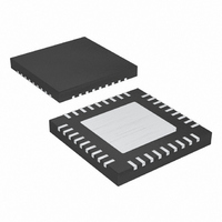
MAX8798ETX+ Maxim Integrated Products, MAX8798ETX+ Datasheet - Page 27

MAX8798ETX+
Manufacturer Part Number
MAX8798ETX+
Description
IC INTERNAL-SW BOOST REG 36-TQFN
Manufacturer
Maxim Integrated Products
Datasheet
1.MAX8798ETX.pdf
(31 pages)
Specifications of MAX8798ETX+
Applications
LCD Monitor, Notebook Display
Current - Supply
400µA
Voltage - Supply
1.8 V ~ 6 V
Operating Temperature
-40°C ~ 85°C
Mounting Type
Surface Mount
Package / Case
36-TQFN Exposed Pad
Operating Supply Voltage
1.8 V to 5.5 V
Maximum Operating Temperature
- 40 C
Mounting Style
SMD/SMT
Maximum Power Dissipation
2179.8 mW
Minimum Operating Temperature
+ 85 C
Supply Current
4 uA
Input Voltage
4V
Output Current
400mA
Output Voltage
18V
No. Of Outputs
2
Power Dissipation Pd
2.18W
Supply Voltage Range
1.8V To 5.5V
No. Of Pins
36
Operating Temperature Range
-40°C To +85°C
Rohs Compliant
Yes
Lead Free Status / RoHS Status
Lead free / RoHS Compliant
Careful PCB layout is important for proper operation.
Use the following guidelines for good PCB layout:
•
•
Integrated 3-Channel Scan Driver for TFT LCDs
Minimize the area of high-current loops by placing
the inductor, output diode, and output capacitors
near the input capacitors and near LX and PGND.
The high-current input loop goes from the positive
terminal of the input capacitor to the inductor, to the
IC’s LX pin, out of PGND, and to the input capaci-
tor’s negative terminal. The high-current output loop
is from the positive terminal of the input capacitor to
the inductor, to the output diode (D1), to the posi-
tive terminal of the output capacitors, reconnecting
between the output capacitor and input capacitor
ground terminals. Connect these loop components
with short, wide connections. Avoid using vias in
the high-current paths. If vias are unavoidable, use
many vias in parallel to reduce resistance and
inductance.
Create a power ground island (PGND) consisting of
the input and output capacitor grounds, PGND pin,
and any charge-pump components. Connect all
these together with short, wide traces or a small
ground plane. Maximizing the width of the power
ground traces improves efficiency and reduces out-
put-voltage ripple and noise spikes. Create an ana-
log ground plane (AGND) consisting of the AGND
pin, all the feedback-divider ground connections, the
operational-amplifier-divider ground connections,
the COMP capacitor ground connection, the
______________________________________________________________________________________
PCB Layout and Grounding
Internal-Switch Boost Regulator with
•
•
•
•
Refer to the MAX8798 evaluation kit for an example of
proper board layout.
BOOST and VL bypass capacitor ground connec-
tions, and the device’s exposed backside paddle.
Connect the AGND and PGND islands by connect-
ing the PGND pin directly to the exposed backside
paddle. Make no other connections between these
separate ground planes.
Place the feedback-voltage-divider resistors as
close as possible to the feedback pin. The divider’s
center trace should be kept short. Placing the resis-
tors far away causes the FB trace to become an
antenna that can pick up switching noise. Care
should be taken to avoid running the feedback
trace near LX or the switching nodes in the charge
pumps.
Place the IN pin and VL pin bypass capacitors as
close as possible to the device. The ground con-
nections of the IN and VL bypass capacitors should
be connected directly to the AGND pin with a wide
trace.
Minimize the length and maximize the width of the
traces between the output capacitors and the load
for best transient responses.
Minimize the size of the LX node while keeping it
wide and short. Keep the LX node away from the
feedback node and analog ground. Use DC traces
as shield if necessary.
27


