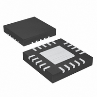
MAX8688ALETG+ Maxim Integrated Products, MAX8688ALETG+ Datasheet - Page 2

MAX8688ALETG+
Manufacturer Part Number
MAX8688ALETG+
Description
IC PWR SUPPLY CTRLR/MONTR 24TQFN
Manufacturer
Maxim Integrated Products
Datasheet
1.MAX8688BHETG.pdf
(38 pages)
Specifications of MAX8688ALETG+
Applications
Power Supply Controller/Monitor
Voltage - Supply
3 V ~ 3.6 V
Current - Supply
6.7mA
Operating Temperature
-40°C ~ 85°C
Mounting Type
Surface Mount
Package / Case
24-TQFN Exposed Pad
Supply Voltage (max)
3.6 V
Supply Voltage (min)
3 V
Operating Temperature Range
- 40 C to + 85 C
Mounting Style
SMD/SMT
Lead Free Status / RoHS Status
Lead free / RoHS Compliant
Voltage - Input
-
Lead Free Status / Rohs Status
Lead free / RoHS Compliant
ABSOLUTE MAXIMUM RATINGS
AVDD, DVDD to AGND .........................................-0.3V to +4.5V
DGND to AGND ..................................................................±0.3V
RS+, RS-, ISN+, ISN- to AGND ................................-0.3V to +6V
RS_C, ISN_C, A1/SCLE, A2/SDAE,
DACOUT to AGND .................................-0.3V to (V
REFO to AGND......................................................-0.3V to +4.5V
Continuous Power Dissipation (T
PACKAGE THERMAL CHARACTERISTICS (Note 2)
ELECTRICAL CHARACTERISTICS
(V
Digital Power-Supply Controller/Monitor
with PMBus Interface
24 TQFN-EP
Note 1: Hand soldering not recommended.
Stresses beyond those listed under “Absolute Maximum Ratings” may cause permanent damage to the device. These are stress ratings only, and functional
operation of the device at these or any other conditions beyond those indicated in the operational sections of the specifications is not implied. Exposure to
absolute maximum rating conditions for extended periods may affect device reliability.
Note 2: Package thermal resistances were obtained using the method described in JEDEC specification JESD51-7, using a four-
2
GENERAL
AVDD/DVDD Operating Range
AVDD and DVDD Operating
Supply Current
AVDD UVLO
OUTPUT-VOLTAGE SENSING
Voltage Regulation Accuracy (2V
Range, Table 8) (Note 4)
Voltage Regulation Accuracy (5.5V
range, Table 8) (Note 4)
RS+, RS- Differential Mode Range
24-Pin TQFN (derate 27.8mW/°C above +70°C)...........2222mW*
A3/ONOFF to AGND............................-0.3V to (V
Junction-to-Ambient Thermal Resistance (θ
Junction-to-Case Thermal Resistance (θ
AVDD
_______________________________________________________________________________________
= V
layer board. For detailed information on package thermal considerations, refer to www.maxim-ic.com/thermal-tutorial.
DVDD
PARAMETER
= 3.3V, T
A
= T
J
A
= -40°C to +85°C, V
= +70°C)
SYMBOL
JC
) ................2.7°C/W
JA
) ............36°C/W
AVDD
AVDD
V
Rising
Hysteresis
MAX8688A, T
V
MAX8688A, T
V
MAX8688B, T
V
MAX8688B, T
V
MAX8688A, T
V
MAX8688A, T
V
MAX8688B, T
V
MAX8688B, T
V
RS+
RS+
RS+
RS+
RS+
RS+
RS+
RS+
RS+
RS+
+ 0.3V)
+ 0.3V)
- V
= V
= 1V, V
= 1V, V
= 1V, V
= 1V, V
= 2.5V, V
= 2.5V, V
= 2.5V, V
= 2.5V, V
RS-
RS-
= 2V, V
= V
RS-
RS-
RS-
RS-
A
A
A
A
A
A
A
A
CONDITIONS
RS-
RS-
RS-
RS-
= 0°C to +85°C,
= -40°C to +85°C,
= 0°C to +85°C,
= -40°C to +85°C,
= 0°C to +85°C,
= -40°C to +85°C,
= 0°C to +85°C,
= -40°C to +85°C,
ISN+
= 0V
= 0V
= 0V
= 0V
SCL, SDA, CLKIO, RST to DGND .........................-0.3V to +4.5V
ENOUT, FLT to DGND..............................................-0.3V to +6V
Thermal Resistance from Junction to Exposed Pad ......2.7°C/W
Operating Temperature .......................................-40°C to +85°C
Junction Temperature ......................................................+150°C
Storage Temperature.........................................-65°C to +150°C
Lead Temperature (soldering, 10s) .................................+300°C
Soldering Temperature (reflow) (Note 1) .........................+260°C
= 0V
= 0V
= 0V
= 0V
RS-
= V
= V
ISN-
AGND
= V
, unless otherwise stated.) (Note 3)
AGND
MIN
2.70
-0.2
-0.3
-0.4
-0.5
-0.3
-0.4
-0.4
-0.5
3.0
0
TYP
100
6.7
2.8
MAX
+0.2
+0.3
+0.4
+0.5
+0.3
+0.4
+0.4
+0.5
2.95
3.6
8.5
5.5
UNITS
mA
mV
%
%
V
V
V


